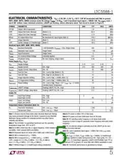
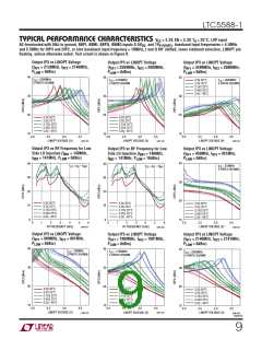
LTC5588-1
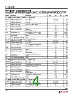
ELECTRICAL CHARACTERISTICS VCC = 3.3V, EN = 3.3V, TA = 25°C, LOP AC-terminated with 50Ω to ground,
BBPI, BBMI, BBPQ, BBMQ common mode DC voltage VCMBB = 0.5VDC, I and Q baseband input signal = 100kHz CW, 1VP-P(DIFF) each, I
and Q 90° shifted, lower sideband selection, LINOPT pin floating, unless otherwise noted. Test circuit is shown in Figure 8.
SYMBOL
OP1dB
OIP2
PARAMETER
CONDITIONS
MIN
TYP
1.9
MAX
UNITS
dBm
Output 1dB Compression
Output 2nd-Order Intercept
Output 3rd-Order Intercept
RF Output Noise Floor
Image Rejection
(Notes 4, 5)
35.4
dBm
OIP3
(Notes 4, 6)
17.9
dBm
NFloor
IR
No Baseband AC Input Signal (Note 3)
(Note 7)
–156.7
–32.3
–30.2
dBm/Hz
dBc
LOFT
Carrier Leakage (LO Feedthrough) (Note 7)
dBm
Baseband Inputs (BBPI, BBMI, BBPQ, BBMQ)
BW
Baseband Bandwidth
Baseband Input Current
Input Resistance
–1dB Bandwidth, R
= 25Ω, Single Ended
SOURCE
430
–136
–3
MHz
μA
kΩ
V
BB
I
Single Ended
b(BB)
R
Single Ended
IN(SE)
CMBB
SWING
V
V
DC Common Mode Voltage
Amplitude Swing
Externally Applied
0.5
No Hard Clipping, Single Ended
0.86
V
P-P
Power Supply (V , V
)
CC1 CC2
V
Supply Voltage
3.15
275
3.3
303
33
3.45
325
900
V
CC
I
I
t
t
t
t
t
Supply Current
EN = High
mA
μA
ns
ns
ns
ns
ns
CC(ON)
CC(OFF)
ON
Supply Current, Sleep Mode
Turn-On Time
EN = 0V
EN = Low to High (Notes 8, 13)
EN = High to Low (Notes 9, 13)
EN = Low to High, <–60dBc (Note 13)
EN = Low to High, <–60dBm (Note 13)
17
Turn-Off Time
10
OFF
Image Rejection Settling
LO Suppression Settling
Phase Settling
80
ON(IR)
ON(LO)
ON(PHASE)
85
EN = Low to High, Phase < 0.5°, f
Constant Board Temperature
= f = 2.14GHz,
RF
70
LOM
V
V
LINOPT Voltage
Floating LINOPT Pin, EN = High
Floating LINOPT Pin, EN = Low
2.56
3.3
V
V
LINOPT(ON)
LINOPT Voltage, Sleep Mode
LINOPT(OFF)
Enable Pin
Enable
Input High Voltage
Input High Current
EN = High
EN = 3.3V
2
V
80
33
nA
Sleep
Input Low Voltage
Input Low Current
EN = Low
EN = 0V
1
V
μA
Temperature Sensor (Thermistor) (Note 14)
R
Thermistor Resistance
Temperature Slope
EN = Low, I = 100μA
1.385
11
kΩ
T
RT
EN = Low, I = 100μA
Ω/°C
RT
Note 1: Stresses beyond those listed under Absolute Maximum Ratings
may cause permanent damage to the device. Exposure to any Absolute
Maximum Rating condition for extended periods may affect device
reliability and lifetime.
Note 2: The LTC5588-1 is guaranteed functional over the operating
temperature range from –40°C to 85°C.
Note 3: At 6MHz offset from the LO signal frequency. 100nF between BBPI
and BBMI, 100nF between BBPQ and BBMQ.
Note 4: Baseband inputs are driven with 4.5MHz and 5.5MHz tones.
Note 8: RF power is within 10% of final value.
Note 9: RF power is at least 30dB down from its ON state.
Note 10: RF matching center frequency is set below band center
frequency in order to align RF passband center frequency with band center
frequency.
Note 11: An external voltage is optimally set at the LINOPT pin for best
output 3rd-order intercept.
Note 12: I and Q baseband Input signal = 10MHz CW, 0.8V
I and Q 0° shifted.
each,
P-P, DIFF
Note 5: IM2 is measured at f – 10MHz.
LO
Note 13: f
= 2.14GHz, P = 0dBm, f = 134MHz; LO feedthrough
LOM BB
LOM
Note 6: IM3 is measured at f – 3.5MHz and f – 6.5MHz.
and image rejection is nulled during previous EN = high cycles, C5 = C6 =
10pF; C13 = 0; Extra 680μF capacitors (SANYO 6SEPC680M) from TP1 to
ground and TP2 to ground, RF noise filter with 93MHz bandwidth is used.
LO
LO
OIP3 = lowest of (1.5 • P{f -5.5MHz} – 0.5 • P{f -6.5MHz})
LO
LO
and (1.5 • P{f -4.5MHz} – 0.5 • P{f -3.5MHz}).
LO
LO
Note 7: Without image or LO feedthrough nulling (unadjusted).
Note 14: Thermistor performance is guaranteed by Design.
55881fb
5

 Linear [ Linear ]