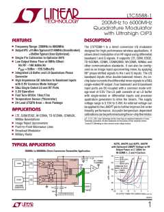
LTC5588-1
ABSOLUTE MAXIMUM RATINGS
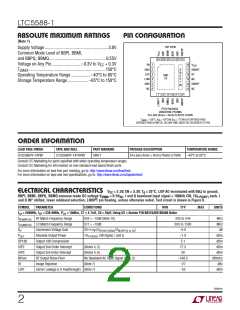
PIN CONFIGURATION
(Note 1)
TOP VIEW
Supply Voltage.........................................................3.8V
Common Mode Level of BBPI, BBMI,
and BBPQ, BBMQ...................................................0.55V
24 23 22 21 20 19
Voltage on Any Pin...........................–0.3V to V + 0.3V
EN
GND
LOP
LOM
GND
NC
1
2
3
4
5
6
18
17
16
V
CC2
CC
G
N
GNDRF
RF
T
JMAX
.................................................................... 150°C
Operating Temperature Range .................–40°C to 85°C
Storage Temperature Range .................. –65°C to 150°C
GND
25
D
R
F
26
15 NC
14 GNDRF
13 NC
7
8
9
10 11 12
PF24 PACKAGE
VARIATION: PF24MA
24-LEAD (4mm s 4mm) PLASTIC UTQFN
T
= 150°C, θ = 43°C/W, θ = 7°C/W (AT EXPOSED PAD)
JA JC
JMAX
EXPOSED PADS (PINS 25, 26) ARE GND, MUST BE SOLDERED TO PCB
ORDER INFORMATION
LEAD FREE FINISH
TAPE AND REEL
PART MARKING
PACKAGE DESCRIPTION
TEMPERATURE RANGE
LTC5588IPF-1#PBF
LTC5588IPF-1#TRPBF
5881T
–40°C to 85°C
24-Lead (4mm × 4mm) Plastic UTQFN
Consult LTC Marketing for parts specified with wider operating temperature ranges.
Consult LTC Marketing for information on non-standard lead based finish parts.
For more information on lead free part marking, go to: http://www.linear.com/leadfree/
For more information on tape and reel specifications, go to: http://www.linear.com/tapeandreel/
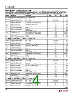
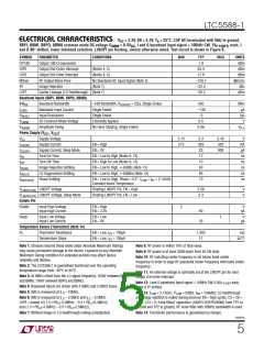
ELECTRICAL CHARACTERISTICS VCC = 3.3V, EN = 3.3V, TA = 25°C, LOP AC-terminated with 50Ω to ground,
BBPI, BBMI, BBPQ, BBMQ common mode DC voltage VCMBB = 0.5VDC, I and Q baseband input signal = 100kHz CW, 1VP-P(DIFF) each, I
and Q 90° shifted, lower sideband selection, LINOPT pin floating, unless otherwise noted. Test circuit is shown in Figure 8.
SYMBOL
PARAMETER
CONDITIONS
MIN
TYP
MAX
UNITS
f
f
f
= 240MHz, f = 239.9MHz, P = 10dBm, C7 = 4.7nH, C8 = 33pF, Using U2 = Anaren P/N B0310J50100A00 Balun
LO
RF
LO
RF Match Frequency Range
LO Match Frequency Range
Conversion Voltage Gain
Absolute Output Power
Output 1dB Compression
Output 2nd-Order Intercept
Output 3rd-Order Intercept
RF Output Noise Floor
S22 < –10dB (Note 10)
S11 < –10dB
200 to 244
200 to 1500
–5.9
MHz
MHz
RF(MATCH)
LO(MATCH)
G
20 • Log (V
/V
)
dB
V
RF(OUT)(50Ω) IN(DIFF)(I or Q)
P
1V
P-P(DIFF)
CW Signal, I and Q
–1.9
dBm
dBm
dBm
dBm
dBm/Hz
dBc
OUT
OP1dB
OIP2
OIP3
NFloor
IR
5.1
(Notes 4, 5)
(Notes 4, 6)
77.3
28
No Baseband AC Input Signal (Note 3)
(Note 7)
–168.3
–27
Image Rejection
LOFT
Carrier Leakage (LO Feedthrough) (Note 7)
–53
dBm
55881fb
2

 Linear [ Linear ]