LTC2943
ELECTRICAL CHARACTERISTICS The l denotes the specifications which apply over the full operating
temperature range, otherwise specifications are at TA = 25°C.
SYMBOL
PARAMETER
CONDITIONS
MIN
TYP
MAX
UNITS
t
Minimum Charge Complete (CC)
Pulse Width
1
µs
PCC
2
I C Timing Characteristics
l
l
l
f
t
t
Maximum SCL Clock Frequency
Bus Free Time Between Stop/Start
400
900
kHz
µs
SCL(MAX)
1.3
BUF(MAX)
Minimum Repeated Start Set-Up
Time
600
ns
SU(STA(MIN))
l
l
t
t
t
Minimum Hold Time (Repeated)
Start Condition
600
600
ns
ns
HD(STA(MIN))
SU(STO(MIN))
SU(DAT(MIN))
Minimum Set-Up Time for Stop
Condition
l
l
l
l
Minimum Data Setup Time Input
Minimum Data Hold Time Input
Data Hold Time Input Output
Data Output Fall Time
100
±0
ns
ns
µs
ns
T
T
T
HD(DAT(MIN))
HDDATO
OF
0.3
0.9
300
(Notes 7, 8)
20 + 0.1 • C
B
Note 1. Stresses beyond those listed under Absolute Maximum Ratings
may cause permanent damage to the device. Exposure to any Absolute
Maximum Rating condition for extended periods may affect device
reliability and lifetime.
Note 2. All currents into pins are positive, all voltages are referenced to
GND unless otherwise specified.
See Choosing R
for more information. 1mAh = 3.6C (Coulombs)
Note 5. Deviation of q from its nominal value.
Note 6. The quantization step of the 14-bit ADC in voltage mode,12-bit
ADC in current mode and 11-bit ADC in temperature mode is not the
same as the LSB of the respective combined 16-bit registers. See Voltage,
Current and Temperature Registers section for more information.
and Choosing Coulomb Counter Prescaler M section
SENSE
LSB
+
–
Note 3. I
= I
+ I
. In most operating modes, I
is
SUPPLY
SENSE
SENSE
SUPPLY
+
flowing in SENSE pin. Only during ADC conversions, current is flowing in
SENSE pin as well. Typically, I
Note 7. C = Capacitance of one bus line in pF (10pF ≤ C ≤ 400pF).
B
B
–
–
–
= V
/1±0k during ADC voltage
SENSE
SENSE
Note 8. Guaranteed by design, not subject to test.
Note 9. See Effect of Differential Offset Voltage on Total Charge Error
section.
–
conversion and I
= 20µA during ADC current conversion.
SENSE
Note 4. The equivalent charge of an LSB in the accumulated charge
register depends on the value of R
prescaling factor M:
and the setting of the internal
SENSE
q
LSB
= 0.340mAh • (±0mΩ/R ) • (M/4096)
SENSE
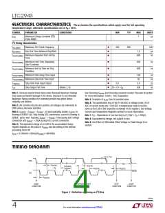
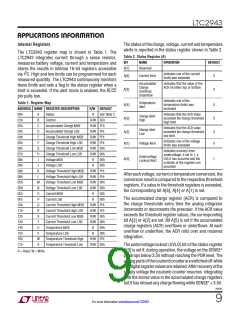
TIMING DIAGRAM
t
OF
SDA
t
BUF
t
SU(DAT)
t
t
t
SU(STA)
HD(DAT0)
HD(DAT1)
t
t
HD(STA)
SU(STO)
2943 TD01
SCL
t
HD(STA)
START
CONDITION
REPEATED START
CONDITION
STOP
CONDITION
START
CONDITION
Figure 1. Definition of Timing on I2C Bus
2943fa
4
For more information www.linear.com/LTC2943

 Linear [ Linear ]