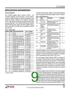
LTC2943
ELECTRICAL CHARACTERISTICS
The l denotes the specifications which apply over the full operating
temperature range, otherwise specifications are at TA = 25°C.
SYMBOL
PARAMETER
CONDITIONS
MIN
TYP
MAX
UNITS
TCE
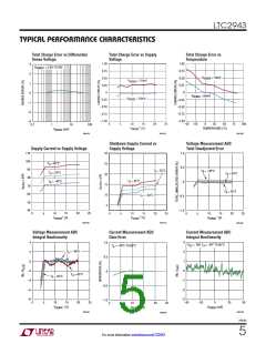
Total Charge Error (Note ±)
10mV ≤ |V
10mV ≤ |V
| ≤ ±0mV DC
| ≤ ±0mV DC
±1
±1.±
±3.±
%
%
%
SENSE
SENSE
l
l
1mV ≤ |V
| ≤ 10mV DC (Note 8)
SENSE
+
l
V
Effective Differential Offset Voltage
(Note 9)
V
≥ ±00µV, V
= 10V
±
10
µV
OSE
SENSE
SENSE
Voltage Measurement ADC
Resolution (No Missing Codes)
Full-Scale Voltage Conversion
l
(Note 8)
14
Bits
V
V
23.6
1.44
FS(V)
ΔV
Quantization Step of 14-Bit Voltage (Note 6)
ADC
mV
LSB
TUE
Voltage Total Unadjusted Error
1
%
%
V
l
l
l
l
l
1.3
Gain
Voltage Gain Accuracy
1.3
±4
±8
48
%
LSB
LSB
ms
V
+
INL
Integral Nonlinearity
V
> ±V
±1
V
SENSE
+
3.6V ≤ V
≤ ±V
SENSE
T
Voltage Conversion Time
CONV(V)
Current Measurement ADC
Resolution (No Missing Codes)
l
l
l
(Note 8)
12
Bits
mV
mV
V
Full-Scale Current Conversion
±60
FS(I)
+
–
V
SENSE
Sense Voltage Differential Input
Range
V
– V
±±0
SENSE
SENSE
ΔI
Quantization Step of 12-Bit Current (Note 6)
ADC
29.3
µV
LSB
Gain
Current Gain Accuracy
1
1.3
%
%
I
l
V
Offset
±1
±1
±10
±4
8
LSB
LSB
ms
OS(I)
l
l
INL
Integral Nonlinearity
Current Conversion Time
I
T
CONV(I)
Temperature Measurement ADC
Resolution (No Missing Codes)
Full-Scale Temperature
l
(Note 8)
11
Bits
K
T
±10
FS
ΔT
Quantization Step of 11-Bit
Temperature ADC
(Note 6)
0.2±
K
LSB
+
TUE
Temperature Total Unadjusted Error
V
≥ ±V
±3
±±
K
K
T
SENSE
l
l
(Note 8)
T
Temperature Conversion Time
8
ms
CONV(T)
Digital Inputs and Digital Outputs
+
l
l
V
V
V
Logic Input Threshold
V
≥ ±V
0.8
0.±
2.2
1.8
0.4
V
V
V
ITH(HV)
ITH(LV)
OL
SENSE
+
3.6V < V
< ±V
SENSE
+
Low Level Output Voltage, ALCC,
SDA
I = 3mA, V
≥ ±V
SENSE
l
l
I
Input Leakage, ALCC, SCL, SDA
V
= ±V
IN
1
µA
pF
IN
C
Input Capacitance, ALCC, SCL, SDA (Note 8)
10
IN
2943fa
3
For more information www.linear.com/LTC2943

 Linear [ Linear ]