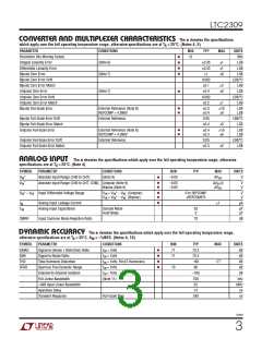
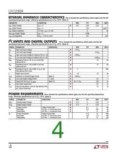
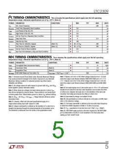
LTC2309
PIN FUNCTIONS
CH3-CH7 (Pins 1-5): Channel 3 to Channel 7 Analog
Inputs. CH3-CH7 can be configured as single-ended
or differential input channels. See the Analog Input
Multiplexer section.
AD1 (Pin 15): Chip Address Control Pin. This pin
is configured as a three-state (Low, High, Floating)
2
address control bit for the device I C address. See
Table 2 for address selection.
2
COM (Pin 6): Common Input. This is the reference
point for all single-ended inputs. It must be free of
noise and should be connected to ground for unipolar
conversions and midway between GND and REFCOMP
for bipolar conversions.
SCL (Pin 16): Serial Clock Pin of the I C Interface. The
LTC2309 can only act as a slave and the SCL pin only
accepts an external serial clock. Data is shifted into
the SDA pin on the rising edges of the SCL clock and
output through the SDA pin on the falling edges of the
SCL clock.
V
(Pin 7): 2.5V Reference Output. Bypass to GND
REF
2
with a minimum 2.2μF tantalum capacitor or low ESR
ceramic capacitor. The internal reference may be over-
driven by an external 2.5V reference at this pin.
SDA (Pin 17): Bidirectional Serial Data Line of the I C
Interface. In transmitter mode (Read), the conversion
result is output at the SDA pin, while in receiver mode
(Write), the D word is input at the SDA pin to con-
IN
REFCOMP (Pin 8): Reference Buffer Output. Bypass to
GND with a 10μF tantalum and 0.1μF ceramic capaci-
tor in parallel. Nominal output voltage is 4.096V. The
internal reference buffer driving this pin is disabled by
figure the ADC. The pin is high impedance during the
data input mode and is an open-drain output (requires
an appropriate pull-up device to V ) during the data
CC
output mode.
grounding V , allowing REFCOMP to be overdriven
REF
by an external source.
DV (Pin 21): 5V Digital Supply. The range of DV
DD
DD
is 4.75V to 5.25V. Bypass DV to GND with a 0.1μF
DD
GND (Pins 9-11, Pins 18-20): Ground. All GND pins
must be connected to a solid ground plane.
ceramic and a 10μF tantalum capacitor in parallel.
CH0-CH2 (Pins 22-24): Channel 0 to Channel 2 Analog
Inputs. CH0-CH2 can be configured as single-ended
or differential input channels. See the Analog Input
Multiplexer section.
AV (Pins 12, 13): 5V Analog Supply. The range of
DD
AV is4.75Vto5.25V.BypassAV toGNDwitha0.1μF
DD
DD
ceramic and a 10μF tantalum capacitor in parallel.
AD0 (Pin 14): Chip Address Control Pin. This pin is
GND (Pin 25): Exposed Pad Ground. Must be soldered
directly to ground plane.
configuredasathree-state(Low,High,Floating)address
2
control bit for the device I C address. See Table 2 for
address selection.
2309f
7

 Linear [ Linear ]