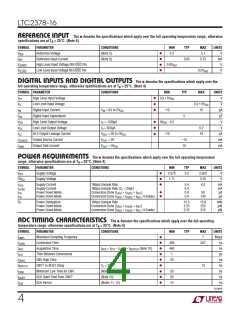
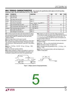
LTC2378-16
pin FuncTions
CHAIN ꢁPin 1x: Chain Mode Selector Pin. When low, the
LTC2378-16 operates in normal mode and the RDL/SDꢁ
input pin functions to enable or disable SDO. When high,
the LTC2378-16 operates in chain mode and the RDL/SDꢁ
pin functions as SDꢁ, the daisy-chain serial data input.
ꢀUSY ꢁPin 11x: ꢀUSY ꢁndicator. Goes high at the start of
a new conversion and returns low when the conversion
has finished. Logic levels are determined by ±V .
DD
RD5/SDI ꢁPin 12x: When CHAꢁI is low, the part is in nor-
mal mode and the pin is treated as a bus enabling input.
When CHAꢁI is high, the part is in chain mode and the
pin is treated as a serial data input pin where data from
another ADC in the daisy-chain is input. Logic levels are
Logic levels are determined by ±V .
DD
V
ꢁPin 2x: 2.5V Power Supply. The range of V is
DD
DD
2.375Vto2.625V. ꢀypassV toGIDwitha1±µFceramic
DD
capacitor.
determined by ±V .
DD
GND ꢁPins 3, 6, 1± and 16x: Ground.
SCKꢁPin13x:SerialDataClockꢁnput.WhenSDOisenabled,
the conversion result or daisy-chain data from another
ADC is shifted out on the rising edges of this clock MSꢀ
+
–
IN , IN ꢁPins 4, .x: Positive and Iegative Differential
Analog ꢁnputs.
first. Logic levels are determined by ±V .
DD
REF ꢁPin 7x: Reference ꢁnput. The range of REF is 2.5V
to 5.1V. This pin is referred to the GID pin and should be
decoupledcloselytothepinwitha47µFceramiccapacitor
(X5R, ±8±5 size).
SDOꢁPin14x:SerialDataOutput. Theconversionresultor
daisy-chain data is output on this pin on each rising edge
of SCK MSꢀ first. The output data is in 2’s complement
format. Logic levels are determined by ±V .
DD
REF/DGCꢁPin8x:WhentiedtoREF,digitalgaincompression
OV ꢁPin 1.x: ꢁ/O ꢁnterface Digital Power. The range of
DD
isdisabledandtheLTC2378-16definesfull-scaleaccording
OV is 1.71V to 5.25V. This supply is nominally set to
DD
to the ±V analog input range. When tied to GID, digital
REF
the same supply as the host interface (1.8V, 2.5V, 3.3V,
gain compression is enabled and the LTC2378-16 defines
or 5V). ꢀypass OV to GID with a ±.1µF capacitor.
DD
full-scale with inputs that swing between 1±% and 9±%
of the ±V analog input range.
GND ꢁEꢂposed Pad Pin 17 – DFN Package Onlyx: Ground.
Exposedpadmustbesoldereddirectlytothegroundplane.
REF
CNV ꢁPin 9x: Convert ꢁnput. A rising edge on this input
powers up the part and initiates a new conversion. Logic
levels are determined by ±V .
DD
FuncTional block DiagraM
V
= 2.5V
DD
OV = 1.8V to 5V
DD
REF = 5V
LTC2378-16
CHAIN
SDO
RDL/SDI
SCK
+
+
IN
SPI
PORT
16-BIT SAMPLING ADC
–
–
IN
CNV
BUSY
REF/DGC
CONTROL LOGIC
GND
237816 BD01
237816f
8

 LINEAR_DIMENSIONS [ Linear Dimensions ]