LTC2378-16
aDc TiMing characTerisTics The l denotes the specifications which apply over the full operating
temperature range, otherwise specifications are at TA = 2.°C0 ꢁNote 4x
SYMꢀO5
PARAMETER
CONDITIONS
MIN
4
TYP
MAX
UNITS
ns
l
l
l
l
l
l
l
l
l
l
t
t
t
t
t
t
t
t
t
t
SCK High Time
SCKH
SCK Low Time
4
ns
SCKL
(Iote 11)
(Iote 11)
4
ns
SDꢁ Setup Time From SCK↑
SDꢁ Hold Time From SCK↑
SCK Period in Chain Mode
SDO Data Valid Delay from SCK↑
SDO Data Remains Valid Delay from SCK↑
SDO Data Valid Delay from ꢀUSY↓
ꢀus Enable Time After RDL↓
ꢀus Relinquish Time After RDL↑
SSDꢁSCK
HSDꢁSCK
SCKCH
DSDO
1
ns
t
= t
+ t (Iote 11)
DSDO
13.5
ns
SCKCH
SSDꢁSCK
C = 2±pF (Iote 11)
L
9.5
ns
C = 2±pF (Iote 1±)
L
1
ns
HSDO
C = 2±pF (Iote 1±)
L
5
ns
DSDOꢀUSYL
EI
(Iote 11)
(Iote 11)
16
13
ns
ns
DꢁS
Note 1: Stresses beyond those listed under Absolute Maximum Ratings
may cause permanent damage to the device. Exposure to any Absolute
Maximum Rating condition for extended periods may effect device
reliability and lifetime.
Note 7: ꢀipolar zero-scale error is the offset voltage measured from
–±.5LSꢀ when the output code flickers between ±±±± ±±±± ±±±± ±±±± and
1111 1111 1111 1111. Full-scale bipolar error is the worst-case of –FS
or +FS untrimmed deviation from ideal first and last code transitions and
includes the effect of offset error.
Note 2: All voltage values are with respect to ground.
Note 8: All specifications in dꢀ are referred to a full-scale ±5V input with a
5V reference voltage.
Note 3: When these pin voltages are taken below ground or above REFor
OV , they will be clamped by internal diodes. This product can handle
DD
input currents up to 1±±mA below ground or above REFor OV without
latch-up.
Note 9: f
= 1MHz, ꢁ varies proportionately with sample rate.
SMPL REF
DD
Note 1±: Guaranteed by design, not subject to test.
Note 11: Parameter tested and guaranteed at OV = 1.71V, OV = 2.5V
Note 4: V = 2.5V, OV = 2.5V, REF = 5V, V = 2.5V, f
= 1MHz,
DD
DD
CM
SMPL
DD
DD
REF/DGC = V
.
REF
and OV = 5.25V.
DD
Note .: Recommended operating conditions.
Note 12: t
of 1±ns maximum allows a shift clock frequency up to
SCK
Note 6: ꢁntegral nonlinearity is defined as the deviation of a code from a
straight line passing through the actual endpoints of the transfer curve.
The deviation is measured from the center of the quantization band.
1±±MHz for rising capture.
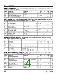
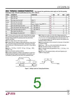
0.8*OV
DD
t
WIDTH
0.2*OV
DD
50%
50%
t
t
DELAY
DELAY
237816 F01
0.8*OV
0.8*OV
0.2*OV
DD
DD
DD
0.2*OV
DD
Figure 10 Voltage 5evels for Timing Specifications
237816f
5

 LINEAR_DIMENSIONS [ Linear Dimensions ]