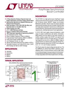
LTC3787
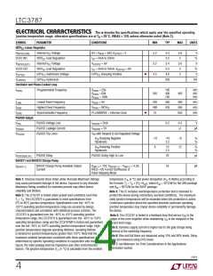
ELECTRICAL CHARACTERISTICS The l denotes the specifications which apply over the specified operating
junction temperature range, otherwise specifications are at TA = 25°C, VBIAS = ±2V, unless otherwise noted (Note 2).
SYMBOL
PARAMETER
CONDITIONS
MIN
5.2
5.2
4.5
TYP
MAX
UNITS
INTV Linear Regulator
CC
INTVCC(VIN)
V
Internal V Voltage
6V < V
< 38V, V = 0
EXTVCC
5.4
0.5
5.4
0.5
4.8
250
5.6
2
V
%
V
CC
BIAS
VLDO INT
INTV Load Regulation
I
CC
= 0mA to 50mA
CC
V
Internal V Voltage
V = 6V
EXTVCC
5.6
2
INTVCC(EXT)
CC
VLDO EXT
INTV Load Regulation
I
CC
= 0mA to 40mA, V = 6V
EXTVCC
%
V
CC
l
V
V
EXTV Switchover Voltage
EXTV Ramping Positive
5
EXTVCC
LDOHYS
CC
CC
EXTV Hysteresis
mV
CC
Oscillator and Phase-Locked Loop
f
Programmable Frequency
R
FREQ
R
FREQ
R
FREQ
= 25k
= 60k
= 100k
105
400
760
kHz
kHz
kHz
PROG
335
465
f
f
f
Lowest Fixed Frequency
Highest Fixed Frequency
Synchronizable Frequency
V
V
= 0V
320
488
75
350
535
380
585
850
kHz
kHz
kHz
LOW
HIGH
SYNC
FREQ
FREQ
= INTV
CC
l
PLLIN/MODE = External Clock
PGOOD Output
V
PGOOD Voltage Low
PGOOD Leakage Current
PGOOD Trip Level
I
= 2mA
= 5V
0.2
0.4
1
V
PGL
PGOOD
I
V
ꢀA
PGOOD
PGOOD
V
V
with Respect to Set Regulated Voltage
FB
PGOOD
V
Ramping Negative
–12
8
–10
2.5
–8
12
%
%
FB
Hysteresis
V
Ramping Positive
10
2.5
%
%
FB
Hysteresis
t
PGOOD Delay
PGOOD Going High to Low
25
ꢀs
PGOOD(DELAY)
BOOST± and BOOST2 Charge Pump
I
BOOST Charge Pump Available Output
Current
V
= 12V; V
– V = 4.5V;
SW1,2
55
ꢀA
BOOST1,2
SW1,2
BOOST1,2
FREQ = 0V, Forced Continuous or
Pulse-Skipping Mode
Note ±: Stresses beyond those listed under Absolute Maximum Ratings
may cause permanent damage to the device. Exposure to any Absolute
Maximum Rating condition for extended periods may affect device
reliability and lifetime.
temperature (T , in °C) and power dissipation (P , in Watts) according to
A D
the formula: T = T + (P • θ ), where θ = 43°C/W for the QFN package
J
A
D
JA
JA
and θ = 90°C/W for the SSOP package.
JA
Note 3: This IC includes overtemperature protection that is intended to
protect the device during momentary overload conditions. The maximum
rated junction temperature will be exceeded when this protection is active.
Continuous operation above the specified absolute maximum operating
junction temperature may impair device reliability or permanently damage
the device.
Note 2: The LTC3787 is tested under pulsed load conditions such that
T ≈ T . The LTC3787E is guaranteed to meet specifications from
J
A
0°C to 85°C junction temperature. Specifications over the –40°C to
125°C operating junction temperature range are assured by design,
characterization and correlation with statistical process controls. The
LTC3787I is guaranteed over the –40°C to 125°C operating junction
temperature range, the LTC3787H is guaranteed over the –40°C to 150°C
operating temperature range and the LTC3787MP is tested and guaranteed
over the full –55°C to 150°C operating junction temperature range. High
junction temperatures degrade operating lifetimes; operating lifetime
is derated for junction temperatures greater than 125°C. Note that the
maximum ambient temperature consistent with these specifications is
determined by specific operating conditions in conjunction with board
layout, the rated package thermal impedance and other environmental
Note 4: The LTC3787 is tested in a feedback loop that servos V to the
FB
output of the error amplifier while maintaining I at the midpoint of the
TH
current limit range.
Note 5: Dynamic supply current is higher due to the gate charge being
delivered at the switching frequency.
Note 6: Rise and fall times are measured using 10% and 90% levels. Delay
times are measured using 50% levels.
Note 7: see Minimum On-Time Considerations in the Applications
Information section.
factors. The junction temperature (T , in °C) is calculated from the ambient
J
3787fc
4

 Linear Systems [ Linear Systems ]