LTC3226
APPLICATIONS INFORMATION
Programming the Supercapacitor
Termination Voltage (CPO)
Programming the Input Voltage Threshold for the
Power-Fail Comparator
The termination voltage of the supercapacitor stack on
the CPO pin can be programmed for any voltage between
2.5V to 5.3V by using a resistor divider from the CPO pin
to GND via the CPO_FB pin such that:
The input voltage threshold below which the power-fail
status pin PFO indicates a power-fail condition and the
LTC3226switchestheinternalLDOoncanbeprogrammed
by using a resistor divider from the V pin to GND via the
IN
PFI pin such that:
⎛
⎜
⎝
⎞
RCP1
RCP2
VCPO = VCPO_FB • 1+
⎛
⎜
⎝
⎞
⎟
RPF1
RPF2
⎠
V
IN(PFO_HI_LO) = VPFI • 1+
⎟
⎠
where V
Typical values for R
to 5M.
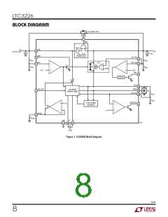
is 1.2V. See the block diagram in Figure 1.
CPO_FB
where V is 1.2V. See Figure 1. Typical values for R
PFI
PF1
and R
are in the range of 40k
CP1
CP2
and R
are in the range of 40k to 5M. For a smooth
PF2
transitionfromnormaltoback-upmode,thePFIthreshold
should be set 50mV to 100mV above the programmed
Programming the Input Current Limit for the Charger
LDO output voltage, V
.
OUT
The input current limit for the LTC3226 charge pump is
programmed by using a single resistor from the PROG
pin to ground. The input current limit is typically 10,500
times the current out of the PROG pin. The PROG pin
voltage always servos to 1V as long as the part is not in
sleep mode. The program resistor and the input current
limit are calculated using the following equations:
The input voltage above which the power-fail status pin
PFO is high impedance and the supercapacitor charger
and the ideal diode are enabled is:
⎛
⎞
RPF1
RPF2
V
= VPFI + VPFI(HYS) • 1+
(
)
IN(PFO_LO_HI)
⎜
⎟
⎝
⎠
1V
IVIN(ILIM)
1V
RPROG
where V
is the hysteresis of the PFI comparator. It
PFI(HYS)
RPROG =10,500•
, IVIN(ILIM) =10,500•
is internally set to a typical value of 20mV.
The hysteresis can be increased externally by adding a
where I
is the input current limit for the charge
VIN(ILIM)
resistor,R ,inserieswithadiode,D1,betweenthePFOand
H
pump charger. The maximum allowable input current limit
of 315mA can be achieved by using a PROG resistor of
33.2k. To maximize the charge transfer rate, the charge
pumpoperatesin1xmodewhenthesupercapacitorvoltage
is less than the input voltage and the charge current out of
CPO pin is only limited by the programmed input current
limit. However, in 2x mode, the average charge current is
approximately half the input current limit.
PFI pins as shown in Figure 2. This network will increase
the low-to-high V threshold for PFO while keeping the
IN
high-to-low threshold intact. The increase in hysteresis
at the input can be calculated as shown:
RPF1
RH
ΔV
= VPFI + VPFI(HYS) – V •
(
)
IN(HYS)
F
3226fa
11

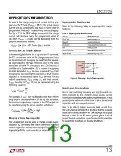
 Linear Systems [ Linear Systems ]