LTC3226
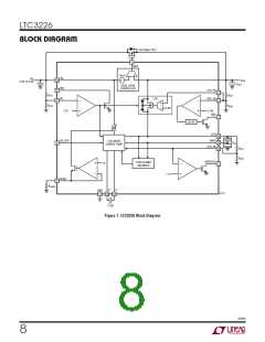
OPERATION
CAPGOOD Status Output
threshold voltage. In backup mode, the charge pump
shuts off and the LDO powers the load as long as there
is enough charge stored on the supercapacitors. The PFI
threshold voltage is programmed by an external resistor
divider via the PFI pin. The output of the PFI comparator
also drives the gate of an open-drain NMOS to report the
status via the PFO pin. In normal mode, the PFO pin is
high Impedance but in backup mode, the pin is pulled
down to ground.
The LTC3226 charge pump includes a comparator to re-
port the status of the supercapacitors via an open-drain
NMOS transistor on the CAPGOOD pin. This pin is pulled
to ground until the CPO pin voltage rises to within 7.5%
of the programmed value. Once the CPO pin is above this
threshold, the CAPGOOD pin goes high impedance.
PROG Pin Short-Circuit Protection
Typically the maximum current that the LTC3226 charge
pump can deliver is set by the PROG resistor. However, if
for any reason, the PROG pin gets shorted to GND, or the
user chooses a PROG resistor value which is far smaller
than recommended, the charge pump input current is
limited to an internally set value of approximately 600mA.
Also the maximum current that can be sourced from the
PROGpinislimitedbyaninternalresistortolessthan1mA.
IDEAL DIODE CONTROLLER
The LTC3226 contains an ideal diode controller which
controls the gate of an external PFET connected between
the input, V , and the output, V , through the GATE
IN
OUT
pin. Under normal operating conditions, this external FET
constitutes the main power path from input to output. For
very light loads, the controller maintains a 15mV delta
across the FET between the input and output voltage. In
the event V suddenly drops below V , the controller
IN
OUT
LOW DROPOUT REGULATOR (LDO)
quicklyturnstheFETcompletelyofftopreventanyreverse
Another principal circuit component of the LTC3226 is the
low dropout regulator (LDO) which transfers power from
conduction from V back to the input supply.
OUT
the supercapacitor stack to V
through a pass element
OUT
RESET COMPARATOR
The LTC3226 contains a RESET comparator which moni-
tors V under all operating modes via the RST_FB pin
with an R
of approximately 200mΩ. This LDO has
DS(ON)
a current limit internally set to 4A. In the event that the
input supply voltage falls below the PFI threshold, the PFI
comparator promptly turns on the LDO to supply the nec-
OUT
and reports the status via an open-drain NMOS transis-
essary load without letting the V
rail droop too much.
tor on the RST pin. At any time, if V
falls 7.5% from
OUT
OUT
However, to prevent unrestricted current flow from the
its programmed value, it pulls the RST pin low almost
input to the supercapacitors through the ideal diode, the
instantaneously.However,ontherisingedgethecompara-
LDO is turned off until the CPO voltage is greater than V
tor waits 290ms after V
crosses the threshold before
IN
OUT
by100mVtypical. TheLDOoutputvoltageisprogrammed
making the RST pin high impedance.
through an external resistor divider via the LDO_FB pin.
GLOBAL THERMAL SHUTDOWN
POWER-FAIL (PFI) COMPARATOR
The LTC3226 includes a global thermal shutdown which
shuts down the entire part in the event the die temperature
exceeds 152°C. It resumes normal operation once the
temperaturedropsbyabout15°Ctoapproximately137°C.
The LTC3226 contains a fast comparator which switches
the part from normal to backup mode in the event the
input voltage, V , falls below an externally programmed
IN
3226fa
10

 Linear Systems [ Linear Systems ]