LTC4060
The ● indicates specifications which apply over the full operating
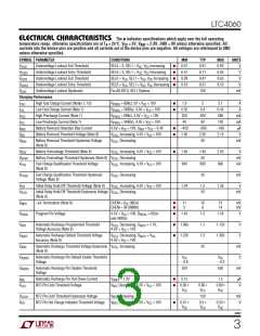
ELECTRICAL CHARACTERISTICS
temperature range, otherwise specifications are at TA = 25°C. VCC = 5V, VBAT = 2.8V, GND = 0V unless otherwise specified. All
currents into the device pins are positive and all currents out of the device pins are negative. All voltages are referenced to GND
unless otherwise specified.
SYMBOL PARAMETER
CONDITIONS
MIN
TYP
100
MAX
UNITS
mV
V
V
NTC Pin Hot Charge Initiation Hysteresis Voltage
NTC Pin Hot Charge Cutoff Threshold Voltage
V
V
Increasing
HTIH
HTC
NTC
NTC
Decreasing, 4.5V ≤ V ≤ 10V
●
●
●
0.37 •
0.4 •
0.43 •
V
CC
V
V
V
CC
CC
CC
V
V
NTC Pin Hot Charge Cutoff Hysteresis Voltage
NTC Pin Disable Threshold Voltage
NTC Pin Pull-Down Current
V
Increasing
100
mV
mV
µA
%
HTCH
NDIS
NTC
25
250
1.5
15
I
t
V
= 2.5V
0.15
–15
NL
ACC
NTC
Timer Accuracy
R
PROG
R
PROG
= 698Ω, C
= 3480Ω, C
= 1.2nF and
= 470pF
0
TIMER
TIMER
Output Drivers
I
Drive Pin Sink Current
V
V
= 4V
40
70
120
mA
Ω
DRV
DRIVE
DRIVE
R
Drive Pin Resistance to V
= 4V, Not Charging
= 10mA
4700
DRV
OL
CC
V
ACP, CHRG Output Pins Low Voltage
I
= I
0.8
2
V
ACP
CHRG
I
ACP, CHRG Output Pins High Leakage Current
Outputs Inactive, V
= V
= V
CC
–2
µA
OH
CHRG
ACP
Control Inputs
V
SHDN, SEL0, SEL1, CHEM, PAUSE Pins Digital
Input Threshold Voltage
V
= 10V
350
650
mV
mV
µA
IT
CC
V
SHDN, SEL0, SEL1, CHEM, PAUSE Pins Digital
Input Hysteresis Voltage
50
ITH
IPD
IPU
I
I
SHDN, SEL0, SEL1, CHEM Pins Digital Input
Pull-Down Current
V
V
= 10V, V = V
0.4
–2
2
CC
IN
IN
CC
PAUSE Pin Digital Input Pull-Up Current
= GND
–0.4
µA
Note 1: Absolute Maximum Ratings only indicate limits for survivability.
Operating the device beyond these limits may result in permanent damage.
Continuous or extended application of these maximum levels may
adversely affect device reliability.
Note 2: The LTC4060 is guaranteed to meet performance specifications
from 0°C to 70°C ambient temperature range and 0°C to 85°C junction
temperature range. Specifications over the –40°C to 85°C operating
ambient temperature range are assured by design, characterization and
correlation with statistical process controls.
Note 3: This IC includes overtemperature protection that is intended to
protect the device during momentary overload conditions. Overtempera-
ture protection is activated at a temperature of approximately 145°C,
which is above the specified maximum operating junction temperature.
Continuous operation above the specified maximum operation temperature
may result in device degradation or failure. Operating junction temperature
Note 5: Assumes that the external PNP pass transistor has negligible B-C
reverse leakage current when the collector is biased at 2.8V (V for two
BAT
charged cells in series) and the base is biased at V
.
CC
Note 6: Assumes that the external PNP pass transistor has negligible B-E
reverse leakage current when the emitter is biased at 0V (V ) and the
CC
base is biased at 5.6V (V for four charged cells in series).
BAT
Note 7: The charge current specified is the regulated current through the
internal current sense resistor that flows into the external PNP pass
transistor’s emitter. Actual battery charging current is slightly less and
depends upon PNP alpha.
Note 8: Given as a per cell voltage (V /Number of Cells).
BAT
Note 9: Supply current includes the current programming resistor current
of 2mA. The charger is paused and not charging the battery.
Note 10: The minimum V supply is set at 5V during this test to
CC
compensate for voltage drops due to test socket contact resistance and 2A
of current. This ensures that the supply voltage delivered to the device
under test does not fall below the UVLO entry threshold. Specification at
T (in °C) is calculated from the ambient temperature T and the average
J
A
power dissipation P (in watts) by the formula:
D
T = T + θ • P
D
J
A
JA
the minimum V of 4.5V is assured by design and characterization.
CC
Note 4: Short duration drops below the minimum V specification of
CC
several microseconds or less are ignored by the undervoltage detection
circuit.
4060f
4

 Linear Systems [ Linear Systems ]