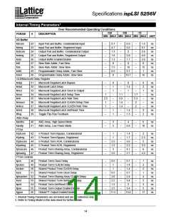
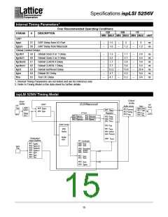
Specifications ispLSI 5256V
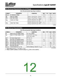
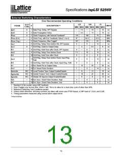
External Switching Characteristics
Over Recommended Operating Conditions
TEST3
COND.
-125
-100
-70
DESCRIPTION 4,5
UNITS
PARAM.
pd1
#
MIN. MAX. MIN. MAX. MIN. MAX.
A
A
1 Data Prop. Delay, 5PT Bypass
—
—
125
87
167
6
7.5
9.5
—
—
—
—
4
—
—
10
13
—
—
—
—
5.5
—
—
—
—
—
70
43.5
83
12
—
0
15
19
—
—
—
—
8
ns
ns
t
t
f
f
f
t
t
t
t
t
2 Data Propagation Delay
pd2
A
3 Clock Frequency with Internal Feedback1
4 Clock Freq. with Ext. Feedback,1/(tsu2 + tco1)
5 Clock Frequency, Max Toggle2
100
64.5
125
8
MHz
MHz
MHz
ns
max
—
—
—
A
max (Ext.)
max (Tog.)
su1
6 GLB Reg. Setup Time before Clk, 5PT bypass
7 GLB Reg. Clock to Output Delay
—
0
—
ns
co1
—
—
—
8 GLB Reg. Hold Time after Clock, 5PT bypass
9 GLB Reg. Setup Time before Clock
10 GLB Reg. Hold Time after Clock
—
—
—
0
—
—
—
ns
h1
7.5
0
10
0
15
0
ns
su2
ns
h2
GLB Reg. Setup Time before Clock, Input Reg.
Path
—
11
6
—
8
—
12
—
ns
tsu3
—
A
12 GLB Reg. Hold Time after Clock, Input Reg. Path
13 Ext. Reset Pin to Output Delay
0
—
7
—
15
—
9
0
—
9
—
20
—
12
24
8
0
—
14
—
—
—
6
—
30
—
18
30
12
—
—
ns
ns
ns
ns
ns
ns
ns
ns
t
t
t
t
t
t
t
t
h3
r1
—
14 Ext. Reset Pulse Duration
rw1
B/C 15 Local Product Term Output Enable/Disable
B/C 16 Global Product Term Output Enable/Disable
B/C 17 Global OE Input to Output Enable/Disable
—
—
—
3
—
—
—
4
ptoe/dis
gptoe/dis
goe/dis
wh
18
6
—
—
18 Ext. Sync. Clock Pulse Duration, High
19 Ext. Sync. Clock Pulse Duration, Low
—
—
—
—
3
4
6
wl
1. Standard 32-bit counter using GRP feedback.
2. fmax (Toggle) may be less than 1/(twh + twl). This is to allow for a clock duty cycle of other than 50%.
3. Reference Switching Test Conditions section.
4. Unless noted otherwise, all timing numbers are taken with worst case PTSA fanout, a GRP load of 1 GLB, and CLK0.
5. Timing parameters measured using normal active output driver.
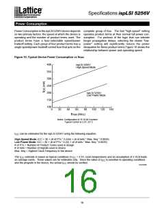
Timing Ext.5256.eps
13

 LATTICE [ LATTICE SEMICONDUCTOR ]