King Billion Electronics Co., Ltd
HE84770
駿 億 電 子 股 份 有 限 公 司
HE80000 SERIES
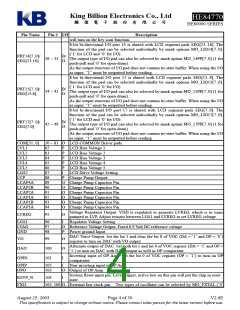
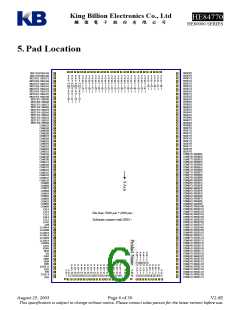
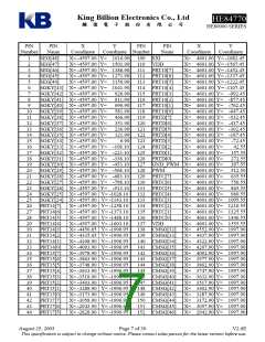
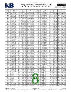
Pin Name
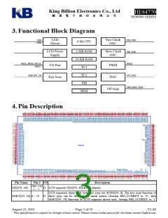
FXI
Pin # I/O
Description
B
for RC type and ‘1’ for crystal type). For RC type oscillator, one resistor need to be
connected between FXI and GND. For crystal oscillator, one crystal need to be placed
between FXI and FXO. Please refer to application circuit for details.
Test input pin. Please bond this pad and reserve a test point on PCB for debugging.
But for improving ESD, please connect this point with zero Ohm resistor to GND.
External slow clock pins. Slow clock is clock source for LCD display, TIMER1,
TSTP_P
107
I
SXO,
SXI
O, Time-Base and other internal blocks. Both crystal and RC oscillator are provided. The
108, 109
110
I
slow clock type can be selected by mask option MO_SXTAL. Choose ‘0’ for RC type
and ‘1’ for crystal oscillator.
Positive power Input. 0.1 µF decoupling capacitors should be placed as close to IC
VDD and GND pads as possible for best decoupling effect.
VDD
P
8-bit bi-directional I/O port 10. The output type of I/O pad can be selected by mask
option MO_10PP[7..0] (‘1’ for push-pull and ‘0’ for open-drain).
As the output structure of I/O pad does not contain tri-state buffer. When using the I/O
pad as input pad, “1” must be outputted before reading.
111 ~
118
PRT10[7..0]
B
8-bit bi-directional I/O port D. The output type of I/O pad can also be selected by
mask option MO_DPP[7..0] (‘1’ for push-pull and ‘0’ for open-drain).
As the output structure of I/O pad does not contain tri-state buffer. When using the I/O
as input, ‘1’ must be outputted before reading the pin.
119 ~
126
PRTD[7..0]
B
PRTD[7..2] can be used as wake-up pins. PRTD[7..6] can be as external interrupt
sources.
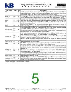
GND_PWM 127
O Dedicated Ground for PWM output.
The PWM output can drive speaker or buzzer directly. Set the bit2 of VOC register as
PWM
128
O
one to turn on PWM. Using VDD & PWM to drive output device.
8-bit bi-directional I/O port C. PRTC[7:4] is shared with Key Scan Dedicated Input
SCNI[3:0]. The Key Scan function can be disabled by clearing MO_LCDKEY mask
option to ‘0’.
129 ~
136
PRTC[7..0]
B
P
The output type of I/O pad can also be selected by mask option MO_CPP[7..0] (‘1’
for push-pull and ‘0’ for open-drain).
As the output structure of I/O pad does not contain tri-state buffer. When using the I/O
as input, ‘1’ must be outputted before reading the pin.
VDD_RAM 137
138 ~
Dedicated power input for RAM
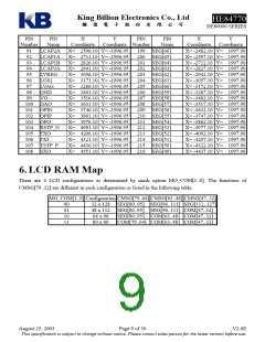
COM[32..79] pads are shared with SEG[127..80] outputs. The functions of the pads to
CMSG[32..79]
O be COM drivers or SEG drivers can be selected by mask option MO_COM[0]. Please
185
refer to LCD driver configuration for details.
I: Input, O: Output, B: Bidirectional, P: Power.
August 25, 2003
Page 5 of 30
V2.6E
This specification is subject to change without notice. Please contact sales person for the latest version before use.

 KB [ King blillion Electronics Co.,Ltd. ]