King Billion Electronics Co., Ltd
HE84770
駿 億 電 子 股 份 有 限 公 司
HE80000 SERIES
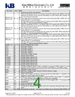
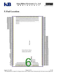
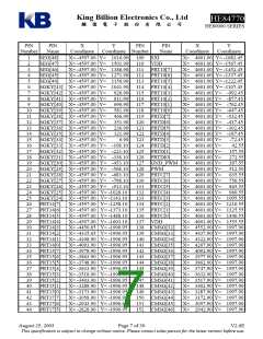
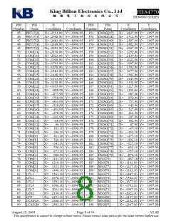
Pin Name
Pin # I/O
Description
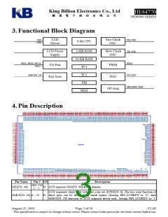
will turn on the key scan function.
8-bit bi-directional I/O port 14 is shared with LCD segment pads SEG[23..16]. The
function of the pad can be selected individually by mask options MO_LIO14[7..0].
(‘1’ for LCD and ‘0’ for I/O).
PRT14[7..0]/
SEG[23:16]
B/
26 ~ 33
O
The output type of I/O pad can also be selected by mask option MO_14PP[7..0] (1 for
push-pull and ‘0’ for open-drain).
As the output structure of I/O pad does not contain tri-state buffer. When using the I/O
as input, “1” must be outputted before reading.
8-bit bi-directional I/O port 15 is shared with LCD segment pads SEG[15..8]. The
function of the pad can be selected individually by mask options MO_LIO15[7..0].
(‘1’ for LCD and ‘0’ for I/O).
PRT15[7..0]/
SEG[15:8]
B/
34 ~ 41
O
The output type of I/O pad can also be selected by mask option MO_15PP[7..0] (1 for
push-pull and ‘0’ for open-drain).
As the output structure of I/O pad does not contain tri-state buffer. When using the I/O
as input, “1” must be outputted before reading.
8-bit bi-directional I/O port 17 is shared with LCD segment pads SEG[7..0]. The
function of the pad can be selected individually by mask options MO_LIO17[7..0].
(‘1’ for LCD and ‘0’ for I/O).
PRT17[7..0]/
SEG[7:0]
B/
42 ~ 49
O
The output type of I/O pad can also be selected by mask option MO_17PP[7..0] (1 for
push-pull and ‘0’ for open-drain).
As the output structure of I/O pad does not contain tri-state buffer. When using the I/O
as input, “1” must be outputted before reading.
COM[31..0] 50 ~ 81 O LCD COMMON Driver pads.
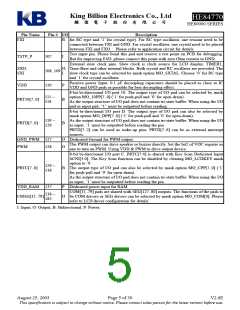
LVL1
82
83
84
85
86
87
88
89
90
91
92
93
94
P
P
P
P
P
I
LCD Bias Voltage 1.
LCD Bias Voltage 2
LCD Bias Voltage 3
LCD Bias Voltage 4
LCD Bias Voltage 5.
LCD Drive Voltage Setting
Charge Pump Output..
LVL2
LVL3
LVL4
LVL5
LGS2
LVP
P
LCAP4A
LCAP2B
LCAP2A
LCAP1A
LCAP1B
LCAP3A
O Charge Pump Capacitor Pin.
O Charge Pump Capacitor Pin.
O Charge Pump Capacitor Pin.
O Charge Pump Capacitor Pin.
O Charge Pump Capacitor Pin.
O Charge Pump Capacitor Pin.
Voltage Regulator Output. VDD is regulated to generate LVREG, which is in turns
LVREG
95
O
pumped to LVP. Adjust resistor between LGS1 and LVREG to set LVREG voltage.
LGS1
LVAG
GND
96
97
98
I
Regulator Voltage Setting
O Reference Voltage Output. Fixed 0.9 Volt DC reference voltage
P
Power ground Input.
DAC Voice Output. Set the bit 1 and clear the bit 0 of VOC (DA = ‘1’ and OP = ‘0’)
register to turn on DAC with VO output.
VO
99
O
Alternate output of DAC. Set both bit 1 and bit 0 of VOC register (DA = ‘1’ and OP =
‘1’) to turn on DAC with DAO output as well as OP comparator.
Inverting input of OP Amp. Set the bit 0 of VOC register (OP = ‘1’) to turn on OP
comparator.
DAO
OPIN
100
101
O
I
I
OPIP
OPO
102
103
Non-inverting input of OP Amp.
O Output of OP Amp.
System Reset input pin. Level trigger, active low on this pin will put the chip in reset
RSTP_N
FXO,
104
I
state.
105, 106 O, External fast clock pin. Two types of oscillator can be selected by MO_FXTAL (‘0’
August 25, 2003
Page 4 of 30
V2.6E
This specification is subject to change without notice. Please contact sales person for the latest version before use.

 KB [ King blillion Electronics Co.,Ltd. ]