IXDN404PI / N404SI / N404SI-16 IXDI404PI / I404SI / I404SI-16
IXDF404PI / F404SI / F404SI-16
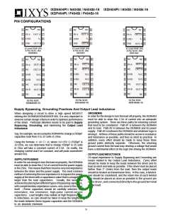
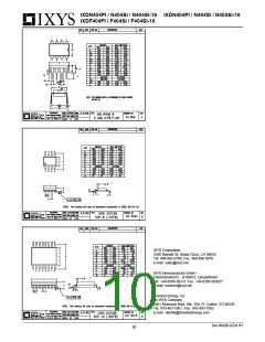
PIN CONFIGURATIONS
1
2
3
4
NC
OUT A
VS
NC
8
7
6
5
1
2
3
4
NC
OUT A
VS
NC
8
7
6
5
1
2
3
4
NC
OUT A
VS
NC
8
7
6
5
IN A
GND
INB
IN A
GND
INB
IN A
GND
INB
OUT B
OUT B
OUT B
8 Lead PDIP (PI)
8 Pin SOIC (SI)
IXDN404
8 Lead PDIP (PI)
8 Pin SOIC (SI)
IXDI404
8 Lead PDIP (PI)
8 Pin SOIC (SI)
IXDF404
NC
NC
1
NC
OUT A
OUT A
VCC
16
15
14
13
12
11
NC 16
1
NC
NC
OUT A
OUT A
VCC
16
15
14
13
12
11
1
2
3
4
5
6
7
8
OUT A
15
14
13
12
11
2
3
4
5
6
7
8
IN A
NC
2
3
4
5
6
7
8
IN A
NC
IN A
NC
OUT A
VCC
GND
GND
GND
GND
NC
VCC
GND
NC
VCC
GND
NC
VCC
OUT B
OUT B
OUT B
IN B
NC
IN B
NC
OUT B 10
NC
OUT B 10
NC
IN B
NC
OUT B 10
NC
9
9
9
16 Pin SOIC
IXDI404SI-16
16 Pin SOIC
IXDF404SI-16
16 Pin SOIC
IXDN404SI-16
Supply Bypassing, Grounding Practices And Output Lead inductance
GROUNDING
When designing a circuit to drive a high speed MOSFET
utilizing the IXDN404/IXDI404/IXDF404, it is very important to
observe certain design criteria in order to optimize performance
of the driver. Particular attention needs to be paid to Supply
Bypassing, Grounding, and minimizing the Output Lead
Inductance.
In order for the design to turn the load off properly, the IXDN404
must be able to drain this 2.5A of current into an adequate
grounding system. There are three paths for returning current
that need to be considered: Path #1 is between the IXDN404
and its load. Path #2 is between the IXDN404 and its power
supply. Path #3 is between the IXDN404 and whatever logic is
driving it. All three of these paths should be as low in resistance
and inductance as possible, and thus as short as practical. In
addition, every effort should be made to keep these three
ground paths distinctly separate. Otherwise, the returning
ground current from the load may develop a voltage that would
have a detrimental effect on the logic line driving the IXDN404.
Say,forexample,weareusingtheIXDN404tochargea2500pF
capacitive load from 0 to 25 volts in 25ns.
Using the formula: I= ∆V C / ∆t, where ∆V=25V C=2500pF &
∆t=25ns, we can determine that to charge 2500pF to 25 volts
in 25ns will take a constant current of 2.5A. (In reality, the
charging current won’t be constant, and will peak somewhere
around 4A).
OUTPUTLEADINDUCTANCE
Of equal importance to Supply Bypassing and Grounding are
issues related to the Output Lead Inductance. Every effort
should be made to keep the leads between the driver and its
load as short and wide as possible. If the driver must be placed
farther than 2” (5mm) from the load, then the output leads
should be treated as transmission lines. In this case, a twisted-
pair should be considered, and the return line of each twisted
pair should be placed as close as possible to the ground pin
ofthedriver,andconnecteddirectlytothegroundterminal
of the load.
SUPPLYBYPASSING
In order for our design to turn the load on properly, the IXDN404
must be able to draw this 2.5A of current from the power supply
in the 25ns. This means that there must be very low impedance
between the driver and the power supply. The most common
method of achieving this low impedance is to bypass the power
supply at the driver with a capacitance value that is a magnitude
larger than the load capacitance. Usually, this would be
achievedbyplacingtwodifferenttypesofbypassingcapacitors,
with complementary impedance curves, very close to the driver
itself. (These capacitors should be carefully selected, low
inductance, low resistance, high-pulse current-service
capacitors). Lead lengths may radiate at high frequency due
to inductance, so care should be taken to keep the lengths of
the leads between these bypass capacitors and the IXDN404
to an absolute minimum.
9

 IXYS [ IXYS CORPORATION ]