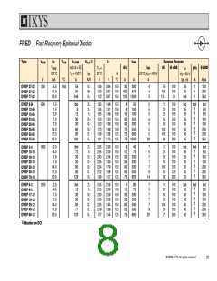
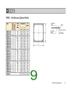
FRED, Rectifier Diode and Thyristor Chips in Planar Design
Fast Recovery Epitaxial Diodes (FRED)
Power switches (IGBT, MOSFET, BJT, GTO) for applications in electronics are only as good as their associated free-wheeling
diodes. At increasing switching frequencies, the proper functioning and efficiency of the power switch, aside from conduction losses,
is determined by the turn-off behavior of the diode (characterized by Qrr, IRM and trr - Fig. 1.
The reverse current character-istic following the peak reverse current IRM is
another very im-portant property. The slope of the decaying reverse current
dirr/dt results from design para- meters (technology and dif-fusion of the
FRED chip Fig. 2. In a circuit this current slope, in conjunction with parasitic
induc-tances (e.g. connecting leads, causes over-voltage spikes and high
frequency interference vol-tages.The higher the dirr/dt ("hard recovery" or
"snap-off" behavior) the higher is the resulting additional stress for both the
diode and the paralleled switch. A slow decay of the reverse current ("soft
recovery" behavior), is the most desirable characteristic, and this is designed
into all FRED. The wide range of available blocking voltages makes it
possible to apply these FRED as output rectifiers in switch-mode power
supplies (SMPS) as well as protective and free-wheeling diodes for power
switches in inverters and welding power supplies.
Fig. 1: Current and voltage during turn-on and
turn-off switching of fast diodes
Glasspassivation
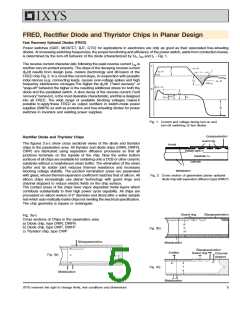
Rectifier Diode and Thyristor Chips
Guard ring
The figures 3 a-c show cross sectional views of the diode and thyristor
Anode
Anode
chips in the passivation area. All thyristor and diode chips (DWN, DWFN,
CWP) are fabricated using separation diffusion processes so that all
Epitaxie Schicht n-
Epitaxy layer n-
junctions terminate on the topside of the chip. Now the entire bottom
surfaces of all chips are available for soldering onto a DCB or other ceramic
substrate without a molybdenum strain buffer. The elimination of the strain
buffer and its solder joint reduces thermal resistance and increases
blocking voltage stability. The junction termination areas are passivated
with glass, whose thermal expansion coefficient matches that of silicon. All
silicon chips increasingly use planar technology with guard rings and
channel stoppers to reduce electric fields on the chip surface.
Substrat n+
Substrate n+
Kathode
Cathode
Metalization
Fig. 2: Cross section of glassivated planar epitaxial
diode chip with seperation diffusion (type DWEP)
The contact areas of the chips have vapor deposited metal layers which
contribute substantially to their high power cycle capability. All chips are
processed on silicon wafers of 5" diameter and diced after a wafer sample
test which auto-matically marks chips not meeting the electrical specification.
The chip geometry is square or rectangular.
Guard ring
Glasspassivation
Fig. 3a-c
Cross sections of Chips in the passivation area
a) Diode chip, type DWN, DWFN
b) Diode chip, type DWP, DWFP
c) Thyristor chip, type CWP
p
n
Fig. 3b)
n+
Glasspassivation
Metalization
Glasspassivation
Emitter
Guard ring
Channel-
Fig. 3a)
stopper
Fig. 3c)
Metalization
Metalization
IXYS reserves the right to change limits, test conditions and dimensions
5

 IXYS [ IXYS CORPORATION ]