Symbols and Definitions
Nomenclature
Cies
Ciss
-di/dt
IC
Input capacitance of IGBT
IGBT and MOSFET Discrete
Input capacitance of MOSFET
Rate of decrease of forward current
DC collector current
IXSD 40N60A
IX
(Example)
IXYS
Die technology
ID
IF
IF(AV)M
IFSM
IGT
IR
IRM
IT
IT(AV)M
Drain current
Forward current of diode
Maximum average forward current at specified Th
Peak one cycle surge forward current
Gate trigger current
E
F
G
S
T
NPT3 IGBT
HiPerFETTM Power MOSFET
Fast IGBT
IGBT with SCSOA capability
Standard Power MOSFET
Unassembled chip (die)
Reverse current
D
Maximum peak recovery current
Forward current of thyristor
Maximum average on-state current of a thyristor
at specified Th
Maximum surge current of a thyristor
Static drain-source on-state resistance
Thermal resistance junction to case
Slope resistance of a thyristor or diode
(for power loss calculations)
Case temperature
40
Current rating, 40 = 40 A
N
P
N-channel type
P-channel type
60
Voltage class, 60 = 600 V
ITSM
RDS(on)
Rthjc
rT
xx
MOSFET
A
Prime RDS(on) for standard MOSFET
Low gate charge die
Low gate charge die, 2nd generation
PolarHTTM Power MOSFET
Linear Mode MOSFET
IGBT
No letter, low VCE(sat)
Or A2, std speed type
Or B2, high speed type
Or C2, very high speed type
Q
Q2
P
Tcase
Th
tfi
Heatsink temperature
Current fall time with inductive load
Junction temperature
L
Tj, T(vj)
--
A
B
C
Tjm, T(vj)m Maximum junction temperature
trr
VCE(sat)
VCES
VDRM
Reverse recovery time of a diode
Collector-emitter saturation voltage
Maximum collector-emitter voltage
Maximum repetitive forward blocking
voltage of thyristor
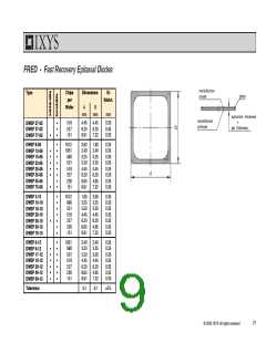
Diode and Thyristor Chips
C-DWEP 69-12
(Diode Example)
VDSS
VF
VR
Drain-source break-down voltage
Forward voltage of diode
Reverse voltage
Maximum peak reverse voltage of thyristor or
diode
C
D
Package type
Chip function
D = Silicon rectifier diode
VRRM
W
Unassembled chip
VT
VT0
On-state voltage of thyristor
Threshold voltage of thyristors or diodes (for
power loss calculation only)
EP
Process designator
EP = Epitaxial rectifier diode
N
P
= Rectifier diode, cathode on top
= Rectifier diode, anode on top
FN = Fast Rectifier diode, cathode on top
FP = Fast Rectifier diode, anode on top
69
Current rating value of one chip in A
Voltage class, 12 = 1200 V
-12
Registration No.:
001947 TS2/765/17557
Registration No.:
001947
W-CWP 55-12/18
(Thyristor Example)
W
C
Package type
Chip and DCB Ceramic Substrates Data book
Edition 2004
Chip function
C = Silicon phase control thyristor
Published by IXYS Semiconductor GmbH
Marketing Communications
Edisonstraße 15, D-68623 Lampertheim
W
P
Unassembled chip
Process designator
P = Planar passivated chip
cathode on top
© IXYS Semiconductor GmbH
All Rights reserved
As far as patents or other rights of third parties are concerned, liability is only
assumed for chips and DCB parts per se, not for applications, processes and
circuits implemented with components or assemblies. Terms of delivery and the
right to change design or specifications are reserved.
55
Current rating value of one chip in A
12/18
Voltage class, 12/18 = 1200 up to 1800 V
© 2004 IXYS All rights reserved
2

 IXYS [ IXYS CORPORATION ]