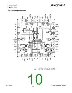
IRS2093MPbF
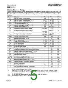
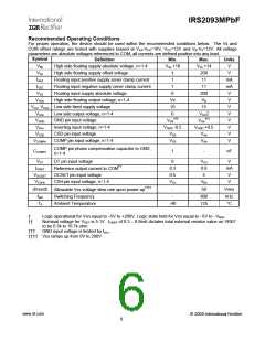
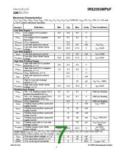
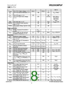
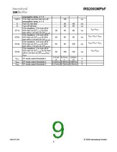
Recommended Operating Conditions
For proper operation, the device should be used within the recommended conditions below. The Vs and
COM offset ratings are tested with supplies biased at VAA-VSS=10V, VCC=12V and VB-VS=12V. All voltage
parameters are absolute voltages referenced to COM; all currents are defined positive into any lead.
Symbol
Definition
Min.
Max.
VSn +14
200
11
Units
V
VBn
High side floating supply absolute voltage, n=1-4
High side floating supply offset voltage
Floating input positive supply zener clamp current
Floating input negative supply zener clamp current
Floating input supply absolute voltage
VSn +10
VSn
†
1
V
IAAZ
mA
mA
V
ISSZ
1
11
VSS
0
200
VB
VHOn
High side floating output voltage, n=1-4
Vs
10
0
V
VCC, VCC2 Low side fixed supply voltage
15
V
VLOn
VGND
VIN-n
Low side output voltage, n=1-4
GND pin input voltage
VCC2
V
†††
VSS
†††
VAA
V
Inverting input voltage, n=1-4
CSD pin input voltage
VGND -0.5
VSS
VGND +0.5
VAA
V
VCSD
V
VCOMPn
COMP pin input voltage, n=1-4
VSS
VAA
V
COMP pin phase compensation capacitor to GND,
n=1-4
CCOMPn
1
-
nF
VDT
IOREF
VOCSET
VCSHn
DT pin input voltage
0
VCC
0.8
5
V
mA
V
Reference output current to COM††
0.3
0.5
VSn
OCSET pin input voltage
CSH pin input voltage, n=1-4
VBn
V
Allowable Vss voltage slew rate upon power-up††††
dVss/dt
-
50
V/ms
kHz
°C
fSW
TA
Switching Frequency
-
800
125
Ambient Temperature
-40
†
Logic operational for Vsn equal to –5V to +200V. Logic state held for Vsn equal to –5V to –VBSn
.
††
Nominal voltage for VREF is 5.1V. IOREF of 0.3 – 0.8mA dictates total external resistor value on VREF
to be 6.3k to 16.7k ohm.
†††
GND input voltage is limited by IIN-n.
†††† Vss ramps up from 0V to 200V.
www.irf.com
© 2009 International Rectifier
6

 INFINEON [ Infineon ]