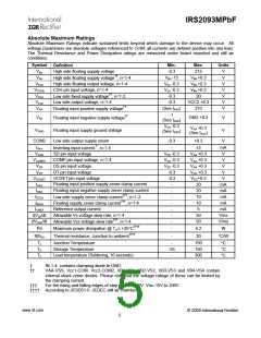
IRS2093MPbF
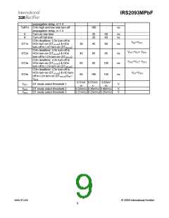
Absolute Maximum Ratings
Absolute Maximum Ratings indicate sustained limits beyond which damage to the device may occur. All
voltage parameters are absolute voltages referenced to COM; all currents are defined positive into any lead.
The Thermal Resistance and Power Dissipation ratings are measured under board mounted and still air
conditions.
Symbol
VBn
Min.
-0.3
Max.
215
Units
Definition
High side floating supply voltage
High side floating supply voltage††, n=1-4
High side floating output voltage, n=1-4
CSH pin input voltage, n=1-4
Low side fixed supply voltage††, n=1-2
Low side output voltage, n=1-4
Floating input positive supply voltage††
V
V
V
V
V
V
V
VSn
VBn -15
VSn -0.3
VSn -0.3
-0.3
VBn +0.3
VBn +0.3
VBn +0.3
20
VHon
VCSHn
VCCn
VLOn
VAA
-0.3
VCC2 +0.3
210
(See IAAZ
)
)
)
-1
Floating input negative supply voltage††
VSS
GND +0.3
V
(See ISSZ
VSS -0.3
(See ISSZ
VAA +0.3
(See IAAZ
VGND
Floating input supply ground voltage
Low side output supply return
Inverting input current †, n=1-4
V
V
)
COM2
-0.3
+0.3
±3
IIN-n
VCSD
-
mA
V
SD pin input voltage
VSS -0.3
VAA +0.3
VAA +0.3
VAA +0.3
VCC +0.3
VCC+0.3
20
VCOMPn
VDS
COMP pin input voltage, n=1-4
DS pin input voltage
VSS -0.3
V
VSS -0.3
V
VDT
DT pin input voltage
-0.3
V
VOCSET
IAAZ
OCSET pin input voltage
Floating input positive supply zener clamp current
-0.3
V
-
-
-
-
-
-
-
mA
mA
mA
mA
mA
V/ns
V/ms
Floating input negative supply zener clamp current
ISSZ
20
Low side supply zener clamp current†††, n=1-2
ICCZn
10
Floating supply zener clamp current†††, n=1-4
Reference output current
IBSZn
10
IOREF
dVSn/dt
dVSSn/dt
5
Allowable Vs voltage slew rate, n=1-4
Allowable Vss voltage slew rate†††, n=1-4
Maximum power dissipation @ TA ≤ +25°C††††
Thermal resistance, Junction to ambient††††
50
50
Pd
-
-
6.2
20
W
RthJA
°C/W
TJ
TS
TL
Junction Temperature
-
-55
-
150
150
300
°C
°C
°C
Storage Temperature
Lead temperature (Soldering, 10 seconds)
†
IN-1-4 contains clamping diode to GND.
††
VAA-VSS, Vcc1-COM, Vcc2-COM2, VB1-VS1, VB2-VS2, VB3-VS3 and VB4-VS4 contain
internal shunt zener diodes. Please note that the voltage ratings of these can be limited by
the clamping current.
†††
For the rising and falling edges of step signal of 10V. Vss=15V to 200V.
†††† According to JESD51-5. JEDEC still air chamber.
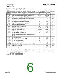
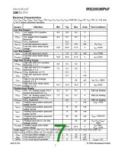
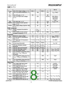
www.irf.com
© 2009 International Rectifier
5

 INFINEON [ Infineon ]