IRS2003(S)PbF
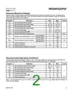
Absolute Maximum Ratings
Absolute maximum ratings indicate sustained limits beyond which damage to the device may occur. All voltage param-
eters are absolute voltages referenced to COM. The thermal resistance and power dissipation ratings are measured
under board mounted and still air conditions.
Symbol
Definition
High-side floating absolute voltage
High-side floating supply offset voltage
High-side floating output voltage
Low-side and logic fixed supply voltage
Low-side output voltage
Min.
Max.
Units
V
B
-0.3
225
V
S
V
- 25
V
+ 0.3
B
B
B
V
HO
V
- 0.3
S
V
+ 0.3
25
V
V
CC
-0.3
-0.3
-0.3
—
V
LO
V
V
+ 0.3
CC
V
IN
Logic input voltage (HIN & ꢀꢁꢂ)
+ 0.3
CC
dV /dt
s
Allowable offset supply voltage transient
50
V/ns
W
(8 Lead PDIP)
(8 Lead SOIC)
(8 Lead PDIP)
(8 Lead SOIC)
—
1.0
0.625
125
200
150
150
P
D
Package power dissipation @ T ≤ +25 °C
A
—
—
Rth
JA
Thermal resistance, junction to ambient
°C/W
—
T
J
Junction temperature
—
T
S
Storage temperature
-55
—
°C
T
L
Lead temperature (soldering, 10 seconds)
300
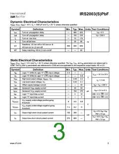
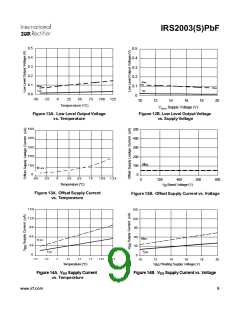
Recommended Operating Conditions
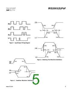
The input/output logic timing diagram is shown in Fig. 1. For proper operation the device should be used within the
recommended conditions. The V offset rating is tested with all supplies biased at a 15 V differential.
S
Symbol
Definition
High-side floating supply absolute voltage
High-side floating supply offset voltage
High-side floating output voltage
Low-side and logic fixed supply voltage
Low-side output voltage
Min.
Max.
Units
V
B
V
+ 10
V + 20
S
S
V
S
Note 1
200
V
HO
V
S
V
B
V
V
CC
10
0
20
V
LO
V
CC
V
IN
Logic input voltage (HIN & ꢀꢁꢂ)
0
V
CC
°C
T
A
Ambient temperature
-40
125
Note 1: Logic operational for V of -5 V to +200 V. Logic state held for V of -5 V to -V . (Please refer to the Design Tip
S
S
BS
DT97-3 for more details).
www.irf.com
2

 INFINEON [ Infineon ]