IRFZ44V
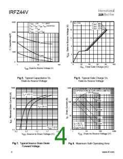
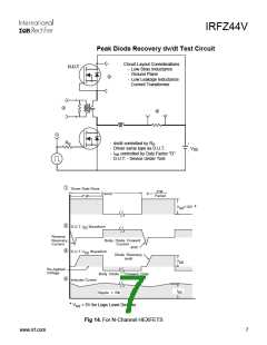
Peak Diode Recovery dv/dt Test Circuit
+
Circuit Layout Considerations
· Low Stray Inductance
· Ground Plane
· Low Leakage Inductance
Current Transformer
D.U.T
-
+
-
-
+
RG
· dv/dt controlled by RG
+
-
· Driver same type as D.U.T.
· ISD controlled by Duty Factor "D"
· D.U.T. - Device Under Test
VDD
Driver Gate Drive
P.W.
P.W.
Period
Period
D =
V
=10V
*
GS
D.U.T. I Waveform
SD
Reverse
Recovery
Current
Body Diode Forward
Current
di/dt
D.U.T. V Waveform
DS
Diode Recovery
dv/dt
V
DD
Re-Applied
Voltage
Body Diode
Forward Drop
Inductor Curent
I
SD
Ripple ≤ 5%
* VGS = 5V for Logic Level Devices
Fig 14. For N-Channel HEXFETS
www.irf.com
7

 INFINEON [ Infineon ]