IRFPS3815
Electrical Characteristics @ TJ = 25°C (unless otherwise specified)
Parameter
Min. Typ. Max. Units
150 ––– –––
Conditions
VGS = 0V, ID = 250µA
V(BR)DSS
Drain-to-Source Breakdown Voltage
V
∆V(BR)DSS/∆TJ Breakdown Voltage Temp. Coefficient ––– 0.18 ––– V/°C Reference to 25°C, ID = 1mA
RDS(on)
VGS(th)
gfs
StaticDrain-to-SourceOn-Resistance
GateThresholdVoltage
––– ––– 0.015
Ω
V
S
VGS = 10V, ID = 63A
VDS = 10V, ID = 250µA
VDS = 50V, ID = 58A
VDS = 100V, VGS = 0V
VDS = 80V, VGS = 0V, TJ = 150°C
VGS = 30V
3.0
47
––– 5.0
Forward Transconductance
––– –––
––– ––– 25
––– ––– 250
––– ––– 100
––– ––– -100
––– 260 390
IDSS
Drain-to-Source Leakage Current
µA
nA
Gate-to-Source Forward Leakage
Gate-to-Source Reverse Leakage
Total Gate Charge
IGSS
VGS = -30V
Qg
ID = 58A
Qgs
Qgd
td(on)
tr
Gate-to-Source Charge
Gate-to-Drain ("Miller") Charge
Turn-On Delay Time
Rise Time
–––
––– 150 230
––– 22 –––
––– 130 –––
53
80
nC VDS = 120V
VGS = 10V
VDD = 75V
ID = 58A
ns
td(off)
tf
Turn-Off Delay Time
Fall Time
–––
–––
51 –––
60 –––
RG = 1.03Ω
VGS = 10V
D
Between lead,
5.0
LD
LS
Internal Drain Inductance
Internal Source Inductance
–––
–––
–––
–––
6mm (0.25in.)
nH
G
from package
13
and center of die contact
S
Ciss
Input Capacitance
––– 6810 –––
––– 1570 –––
––– 480 –––
––– 9820 –––
––– 670 –––
––– 1270 –––
VGS = 0V
Coss
Output Capacitance
pF
VDS = 25V
Crss
Reverse Transfer Capacitance
Output Capacitance
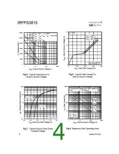
ƒ = 1.0MHz, See Fig. 5
Coss
VGS = 0V, VDS = 1.0V, ƒ = 1.0MHz
VGS = 0V, VDS = 120V, ƒ = 1.0MHz
VGS = 0V, VDS = 0V to 120V
Coss
Output Capacitance
Coss eff.
Effective Output Capacitance ꢀ
Source-Drain Ratings and Characteristics
Parameter
Continuous Source Current
(Body Diode)
Min. Typ. Max. Units
Conditions
D
IS
MOSFET symbol
105
––– –––
showing the
A
G
ISM
Pulsed Source Current
(Body Diode)
integral reverse
––– ––– 390
S
p-n junction diode.
VSD
trr
Diode Forward Voltage
Reverse Recovery Time
Reverse RecoveryCharge
Forward Turn-On Time
––– ––– 1.3
––– 270 410
V
TJ = 25°C, IS = 58A, VGS = 0V
TJ = 25°C, IF = 58A
ns
Qrr
ton
––– 2990 4490 nC di/dt = 100A/µs
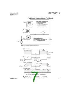
Intrinsic turn-on time is negligible (turn-on is dominated by LS+LD)
Notes:
Repetitive rating; pulse width limited by
Pulse width ≤ 300µs; duty cycle ≤ 2%.
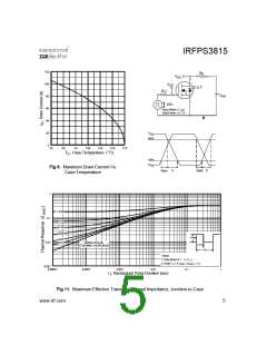
max. junction temperature. (See fig. 11)
ꢀCoss eff. is a fixed capacitance that gives the same charging time
Starting TJ = 25°C, L = 0.96mH
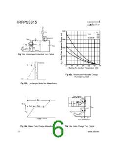
RG = 25Ω, IAS = 58A. (See Figure 12)
as Coss while VDS is rising from 0 to 80% VDSS
ISD ≤ 58A, di/dt ≤ 450A/µs, VDD ≤ V(BR)DSS
TJ ≤ 175°C
,
2
www.irf.com

 INFINEON [ Infineon ]