IRF4905PbF
Electrical Characteristics @ TJ = 25°C (unless otherwise specified)
Parameter
Drain-to-Source Breakdown Voltage
Min. Typ. Max. Units
-55 ––– –––
Conditions
VGS = 0V, ID = -250µA
V(BR)DSS
V
∆V(BR)DSS/∆TJ Breakdown Voltage Temp. Coefficient ––– -0.05 ––– V/°C Reference to 25°C, ID = -1mA
RDS(on)
VGS(th)
gfs
Static Drain-to-Source On-Resistance ––– ––– 0.02
Ω
V
S
VGS = -10V, ID = -38A ꢄ
VDS = VGS, ID = -250µA
VDS = -25V, ID = -38A
VDS = -55V, VGS = 0V
VDS = -44V, VGS = 0V, TJ = 150°C
VGS = 20V
Gate Threshold Voltage
-2.0 ––– -4.0
21 ––– –––
Forward Transconductance
––– ––– -25
––– ––– -250
––– ––– 100
––– ––– -100
––– ––– 180
––– ––– 32
––– ––– 86
IDSS
Drain-to-Source Leakage Current
µA
nA
Gate-to-Source Forward Leakage
Gate-to-Source Reverse Leakage
Total Gate Charge
IGSS
VGS = -20V
Qg
ID = -38A
Qgs
Qgd
td(on)
tr
Gate-to-Source Charge
Gate-to-Drain ("Miller") Charge
Turn-On Delay Time
nC VDS = -44V
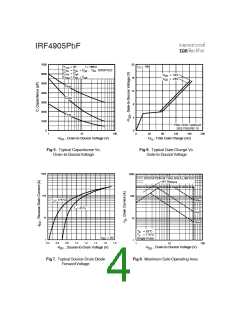
VGS = -10V, See Fig. 6 and 13 ꢄ
–––
–––
–––
–––
18 –––
99 –––
61 –––
96 –––
VDD = -28V
RiseTime
ID = -38A
ns
td(off)
tf
Turn-Off Delay Time
FallTime
RG = 2.5Ω
RD = 0.72Ω, See Fig. 10 ꢄ
Between lead,
6mm (0.25in.)
D
S
4.5
LD
LS
Internal Drain Inductance
Internal Source Inductance
–––
–––
–––
–––
nH
pF
G
from package
7.5
and center of die contact
VGS = 0V
Ciss
Coss
Crss
Input Capacitance
––– 3400 –––
––– 1400 –––
––– 640 –––
Output Capacitance
VDS = -25V
Reverse Transfer Capacitance
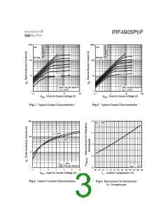
ƒ = 1.0MHz, See Fig. 5
Source-Drain Ratings and Characteristics
Parameter
Continuous Source Current
(Body Diode)
Min. Typ. Max. Units
Conditions
MOSFETsymbol
D
S
IS
-74
––– –––
––– –––
showing the
A
G
ISM
Pulsed Source Current
(Body Diode) ꢀ
integral reverse
-260
p-n junction diode.
VSD
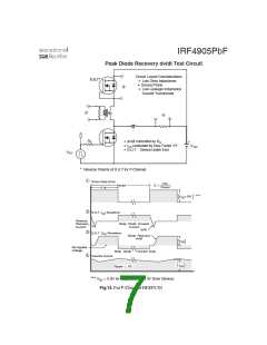
trr
Diode Forward Voltage
Reverse Recovery Time
Reverse Recovery Charge
Forward Turn-On Time
––– ––– -1.6
––– 89 130
––– 230 350
V
TJ = 25°C, IS = -38A, VGS = 0V ꢄ
ns
TJ = 25°C, IF = -38A
Qrr
ton
nC di/dt = -100A/µs ꢄ
Intrinsic turn-on time is negligible (turn-on is dominated by LS+LD)
Notes:
ꢀ Repetitive rating; pulse width limited by
ꢁ ISD ≤ -38A, di/dt ≤ -270A/µs, VDD ≤ V(BR)DSS
TJ ≤ 175°C
,
max. junction temperature. ( See fig. 11 )
ꢂ Starting TJ = 25°C, L = 1.3mH
ꢃ Pulse width ≤ 300µs; duty cycle ≤ 2%.
RG = 25Ω, IAS = -38A. (See Figure 12)

 INFINEON [ Infineon ]