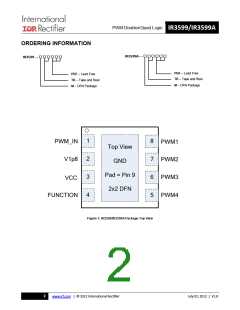
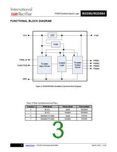
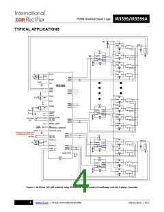
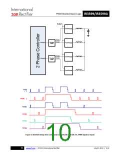
PWM Doubler/Quad Logic
IR3599/IR3599A
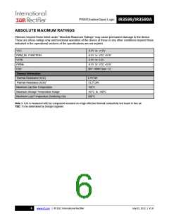
ABSOLUTE MAXIMUM RATINGS
Stresses beyond those listed under “Absolute Maximum Ratings” may cause permanent damage to the device.
These are stress ratings only and functional operation of the device at these or any other conditions beyond those
indicated in the operational sections of the specifications are not implied.
VCC
-0.3V to +4.0V
PWM_IN, FUNCTION
V1P8
-0.3V to VCC +0.3V
-0.3V to 2.2V
PWMx
-0.3V to VCC +0.3V
2KV, HBM Class 1-C
ESD
Thermal Information
Thermal Resistance (ΘJC)
Thermal Resistance (ΘJA)1
Maximum Junction Temperature
Maximum Storage Temperature Range
Maximum Lead Temperature (Soldering 10s)
8.9°C/W
73.2°C/W
150°C
-65°C to 150°C
300°C
Note 1: θJA is measured with the component mounted on a high effective thermal conductivity test board in free air.
TBD: To be determined by Design Engineer.
6
www.irf.com | © 2012 International Rectifier
July 02, 2012 | V1.8

 INFINEON [ Infineon ]