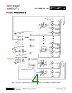
PWM Doubler/Quad Logic
IR3599/IR3599A
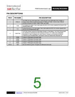
PIN DESCRIPTIONS
PIN #
PIN NAME
PIN DESCRIPTION
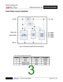
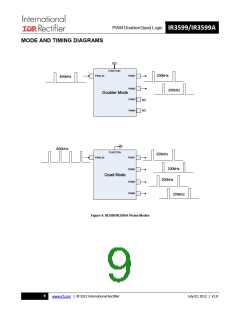
The PWM_IN is the control signal input. Connect this pin to the PWM output of the controller. In
Doubler mode, PWM_IN controls the behavior of PWM1 and PWM2. In QUAD mode, PWM_IN
controls the behavior of PWM1, PWM2, PWM3, and PWM4.
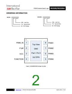
1
PWM_IN
1.8V internal LDO output. Place a high quality low ESR 0.47uF ceramic capacitor from this pin to the
IR3599/IR3599A GND.
2
3
V1p8
VCC
Connect this pin to a +3.3V bias supply. Place a high quality low ESR 0.1uF ceramic capacitor from
this pin to the IR3599/IR3599A GND.
The FUNCTION pin controls the Phase Mode (Doubler or Quad Modes). The FUNCTION pin levels
are controlled by connecting the FUNCTION pin to Ground or VCC. Refer to the configuration
instructions in Table 1 to program the FUNCTION pin. At power up, the function pin selection
is latched into the IR3599/IR3599A, and therefore cannot be changed after initial power up.
4
FUNCTION
5
PWM4
PWM3
PWM2
PWM1
GND
Channel 4 PWM signal to the power stage
6
Channel 3 PWM signal to the power stage
7
8
Channel 2 PWM signal to the power stage
Channel 1 PWM signal to the power stage
(PAD) 9
Bias and reference ground. All signals are referenced to this node.
5
www.irf.com | © 2012 International Rectifier
July 02, 2012 | V1.8

 INFINEON [ Infineon ]