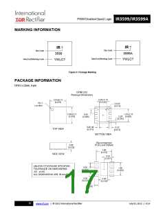
PWM Doubler/Quad Logic
IR3599/IR3599A
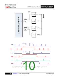
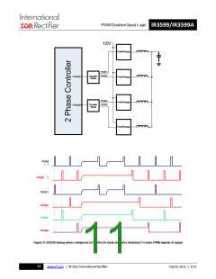
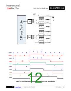
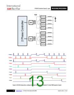
DOUBLER/QUAD MODE REACTION TO
TRI‐STATE PWM INPUT
In Doubler or quad mode, anytime there is a tri-state
on the PWM_IN, all PWM outputs (PWMx) are tri-
stated immediately with minimum delays. When the
PWM_IN transitions from a tri-state to a high and then
from a high to a low, only the 0 deg phase (PWM1)
operates. This allows the VR to operate properly in
PS2 mode and during load releases. Once the
PWM_IN sees a transition from a low to a high, the
doubler or quad function starts again, with output on
the other PWM pins. The tri-state timing when
configured in doubler mode or quad mode are shown
in Figure 5 - Figure 8.
FREQUENCY RANGE
The IR3599/IR3599A is designed to operate
over a wide input and output frequency range.
When operating in Doubler mode, the input frequency
at the PWM_IN input is 2x the output frequency.
When operating in Quad mode, the input frequency
at the PWM_IN input is 4x the output frequency.
The IR3599/IR3599A is designed to operate with
output frequencies between 200 kHz and 800 kHz.
CONFIGURING THE PHASE MODES
The IR3599/IR3599A can operate in 2 separate
Phase modes which are Doubler and Quad. Table 1
shows the user how to configure the Modes utilizing
the FUNCTION pin. The FUNCTION selection (pin 4)
is latched into the IR3599/IR3599A at power up, and
cannot be changed after power on reset.
SUPPLY DECOUPLING CAPACITOR
VCC decoupling to the IR3599/IR3599A is provided
by a 0.1uF bypass capacitor CVcc located close to the
supply input pin. A series resistor Rvcc, typically 10Ω,
is added in series with the supply voltage to filter high
frequency ringing and noise. A 0.47uF bypass
capacitor located close to V1p8 output pin is
recommended for the internal LDO decouple.
15
www.irf.com | © 2012 International Rectifier
July 02, 2012 | V1.8

 INFINEON [ Infineon ]