IR2110(-1-2)(S)PbF/IR2113(-1-2)(S)PbF
Dynamic Electrical Characteristics
V
(V , V , V ) = 15V, C = 1000 pF, T = 25°C and V
= COM unless otherwise specified. The dynamic
BIAS
CC BS DD
L
A
SS
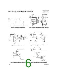
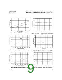
electrical characteristics are measured using the test circuit shown in Figure 3.
Symbol
Definition
Turn-on propagation delay
Turn-off propagation delay
Shutdown propagation delay
Turn-on rise time
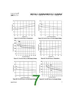
Figure Min. Typ. Max. Units Test Conditions
t
7
8
—
—
—
—
—
120
94
150
125
140
35
V = 0V
S
on
t
V
V
= 500V/600V
= 500V/600V
off
S
t
sd
9
110
25
S
ns
t
r
10
11
t
f
Turn-off fall time
17
25
MT
Delay matching, HS & LS
turn-on/off
(IR2110)
(IR2113)
—
—
—
—
—
—
10
20
Static Electrical Characteristics
V
(V , V , V ) = 15V, T = 25°C and V = COM unless otherwise specified. The V , V and I parameters
BIAS CC BS DD
A
SS
IN TH
IN
are referenced to V and are applicable to all three logic input leads: HIN, LIN and SD. The V and I parameters are
SS
O
O
referenced to COM and are applicable to the respective output leads: HO or LO.
Symbol
Definition
Figure Min. Typ. Max. Units Test Conditions
V
Logic “1” input voltage
12
13
14
15
16
17
18
19
20
9.5
—
—
—
—
—
—
—
—
—
—
—
6.0
1.2
0.1
50
IH
V
IL
Logic “0” input voltage
V
V
OH
High level output voltage, V
Low level output voltage, V
- V
—
I
I
= 0A
= 0A
BIAS
O
O
V
OL
—
O
O
I
Offset supply leakage current
—
V =V = 500V/600V
B S
LK
I
Quiescent V supply current
BS
125
180
15
20
230
340
30
V
= 0V or V
QBS
IN
IN
IN
DD
DD
DD
I
Quiescent V
Quiescent V
supply current
supply current
V
V
= 0V or V
= 0V or V
QCC
CC
DD
µA
I
QDD
I
Logic “1” input bias current
Logic “0” input bias current
40
V
= V
IN DD
IN+
I
21
22
—
—
1.0
9.7
V
IN
= 0V
IN-
V
V
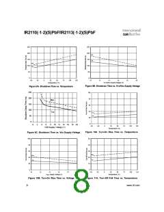
supply undervoltage positive going
BS
7.5
8.6
BSUV+
threshold
V
V
supply undervoltage negative going
23
24
25
26
27
7.0
7.4
7.0
2.0
2.0
8.2
8.5
8.2
2.5
2.5
9.4
9.6
9.4
—
BSUV-
BS
threshold
V supply undervoltage positive going
CC
V
CCUV+
V
threshold
V supply undervoltage negative going
CC
V
CCUV-
threshold
I
Output high short circuit pulsed current
V
O
= 0V, V = V
IN DD
O+
PW ≤ 10 µs
= 15V, V = 0V
O IN
A
I
O-
Output low short circuit pulsed current
—
V
PW ≤ 10 µs
www.irf.com
3

 INFINEON [ Infineon ]