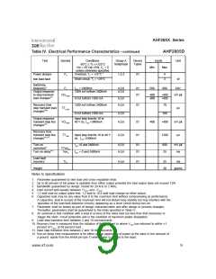
AHF28XX Series
AHF2805D
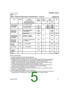
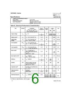
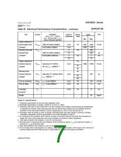
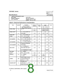
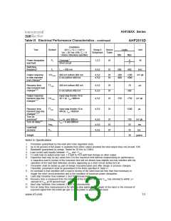
Table IV. Electrical Performance Characteristics - continued
Test
Symbol
Conditions
-55°C Tc +125°C
Group A
Subgroups
Device
Types
Limits
Unit
≤
≤
Vin = 28 Vdc ±5%, CL = 0
unless otherwise specified
Overload, TC = +25°C 8
Min
Max
Power dissipa-
tion load fault
PD
1,2,3
01
6
2
W
Short circuit, TC = +25°C
Switching
frequency4
Output response
to step transient
load changes4,9
FS
IOUT = 2400mA
1200 mA to/from 2400mA
4,5,6
4,5,6
01
01
500
600
kHz
VOTLOAD
-400
-800
+400
+800
mV pk
0 mA to/from 1200 mA
4,5,6
4,5,6
Recovery time
step transient load
changes4,9,10
1200 mA to/from 2400mA
01
70
TTLOAD
µs
0 mA to/from 1200 mA
4,5,6
4,5,6
100
Output response
transient step line
changes4,7,11
Input step from/to 16 to
40 V dc, IOUT =2400mA
VOTLINE
01
01
-400
+400
mV pk
µs
Recovery time
transient step line
changes4,7,10,11
TTLINE
Input step from/to 16 to 40 V
dc, IOUT =2400mA
4,5,6
1200
Turn on
I
OUT =0 and 2400mA
4,5,6
4,5,6
01
01
600
25
mV pk
ms
overshoot4
Turn on delay4,12
VTonOS
TonD
IOUT = 0 and 2400mA
Load fault
recovery7
TrLF
4,5,6
01
25
38
ms
Weight
grams
Notes to Specifications
1. Parameter guaranteed by line load and cross regulation tests.
2. Up to 90 percent of full power is available from either output provided the total output does not exceed 12W.
3. Bandwidth guaranteed by design. Tested for 20 kHz to 2 MHz.
4. Load current split equally between +VOUT and –VOUT
.
5. 1.2 watt load on output under test, 1.2 watt to 10.8 watt load change on other output.
6. Capacitive load may be any value from 0 to the maximum limit without compromising dc performance.
A capacitive load in excess of the maximum limit will not disturb loop stability but may interfere with the
operation of the load fault detection circuitry, appearing as a short circuit during turn-on.
7. Parameter shall be tested as part of design characterization and after design or process changes.
Thereafter, parameters shall be guaranteed to the limits specified in Table IV.
8. An overload is that condition with a load in excess of the rated load but less than that necessary to
trigger the short circuit protection and is the condition of maximum power dissipation.
9. Load step transition time between 2 and 10 microseconds.
10. Recovery time is measured from the initiation of the transient to where VOUT has returned to within ±1
percent of VOUT at 50 percent load.
11. Input step transition time between 2 and 10 microseconds.
12. Turn-on delay time measurement is for either a step application of power at the input or the removal of
a ground signal from the inhibit pin (pin 1) while power is applied to the input.
www.irf.com
9

 INFINEON [ Infineon ]