CA139, CA139A, CA239, CA339, LM339, LM2901, LM3302
Absolute Maximum Ratings
Thermal Information
o
o
Supply Voltage. . . . . . . . . . . . . . . . . . . . . . . . . . . . . . . .36V or ±18V
Differential Input Voltage . . . . . . . . . . . . . . . . . . . . . . . . . . . . . . .36V
Input Voltage . . . . . . . . . . . . . . . . . . . . . . . . . . . . . . . .-0.3V to +36V
Thermal Resistance (Typical, Note 3)
θ
( C/W)
θ
( C/W)
JA
JC
PDIP Package . . . . . . . . . . . . . . . . . . .
SOIC Package . . . . . . . . . . . . . . . . . . .
100
175
N/A
N/A
o
Input Current (V < -0.3V, Note 1) . . . . . . . . . . . . . . . . . . . . . . 50mA
I
Maximum Junction Temperature (Plastic Package). . . . . . . . .150 C
Maximum Storage Temperature Range. . . . . . . . . . -65 C to 150 C
Maximum Lead Temperature (Soldering 10s) . . . . . . . . . . . . 300 C
o
o
Output Short Circuit Duration (Single Supply, Note 2). . .Continuous
o
(SOIC - Lead Tips Only)
Operating Conditions
Temperature Range
CA139, CA139A. . . . . . . . . . . . . . . . . . . . . . . . . . -55 C to 125 C
CA239 . . . . . . . . . . . . . . . . . . . . . . . . . . . . . . . . . . -25 C to 80 C
CA339, LM339 . . . . . . . . . . . . . . . . . . . . . . . . . . . . . 0 C to 70 C
o
o
o
o
o
o
o
o
LM2901, LM3302 . . . . . . . . . . . . . . . . . . . . . . . . . . -40 C to 85 C
CAUTION: Stresses above those listed in “Absolute Maximum Ratings” may cause permanent damage to the device. This is a stress only rating and operation of the
device at these or any other conditions above those indicated in the operational sections of this specification is not implied.
NOTES:
1. Inputs must not go more negative than -0.3V.
2. Short circuits from the output to V+ can cause excessive heating and eventual destruction. The maximum output current independent of V+ is
approximately 20mA.
3. θ is measured with the component mounted on an evaluation PC board in free air.
JA
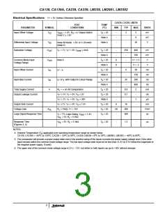
Electrical Specifications V+ = 5V, Unless Otherwise Specified
CA139
CA139A
TEST
CONDITIONS
TEMP
( C)
o
PARAMETER
SYMBOL
MIN
TYP
MAX
MIN
TYP
MAX
UNITS
mV
Input Offset Voltage
V
V
= 1.4V, R = 0,
T = 25
A
-
-
2
-
5
9
-
-
1
-
2
4
IO
REF
Output Switch Point
1.4V
S
Note 4
Note 4
mV
V
Differential Input Voltage
Saturation Voltage
V
-
-
36
-
-
36
V
Keep All Inputs ≥ 0V, or
V- (if used), (Note 5)
ID
V
V - = 1V, V + = 0V,
T = 25
A
-
-
250
400
700
V+ -1.5
V+ -2
25
-
-
250
400
700
V+ -1.5
V+ -2
25
mV
mV
V
SAT
I
I
I
≤ 4mA
SINK
Note 4
-
-
-
-
Common Mode Input
Voltage Range
V
Note 6
T = 25
A
0
0
-
0
0
-
ICR
Note 4
-
-
V
Input Offset Current
Input Bias Current
Total Supply Current
I
I + - I -
T = 25
A
3
3
nA
nA
nA
nA
mA
IO
I
I
Note 4
-
-
100
100
300
2
-
-
100
100
300
2
I
I + or I - with Output in
T = 25
A
-
25
-
-
25
-
IB
I
I
Linear Range
Note 4
-
-
I+
R
= ∞ On All
T = 25
-
0.8
-
0.8
L
A
Comparators
Output Leakage
Current
V + ≥ 1V, V - = 0V,
T = 25
A
-
-
0.1
-
-
1
-
-
-
0.1
-
-
1
-
nA
µA
I
I
V
= 5V
O
V + ≥ 1V, V - = 0V,
Note 4
I
I
V
= 30V
O
Output Sink Current
Voltage Gain
V - ≥ 1V, V + = 0V,
T = 25
6
16
6
16
mA
I
I
A
V
≤ 1.5V
O
A
R
≥ 15kΩ, V+ = 15V
T = 25
-
-
200
300
-
-
50
-
200
300
-
-
V/mV
ns
OL
L
A
Large Signal Response
Time
V = TTL Logic Swing,
T = 25
A
I
V
= 1.4V, V = 5V,
RL
REF
R = 5.1kΩ
L
Response Time
(Figures 3, 4)
V
= 5V, R = 5.1kΩ
T = 25
-
1.3
-
-
1.3
-
µs
RL
L
A
2

 INTERSIL [ Intersil ]