ISL88731C
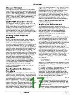
Write To A Register
SLAVE
ADDR + W
REGISTER
ADDR
LO BYTE
DATA
HI BYTE
DATA
S
S
A
A
A
A
A
P
Read From A Register
SLAVE
ADDR + W
REGISTER
ADDR
SLAVE
LO BYTE
DATA
HI BYTE
DATA
A
P
S
A
A
N
P
ADDR + R
S
P
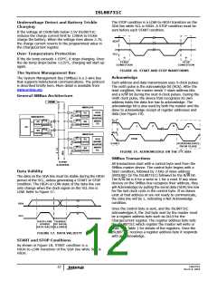
START
STOP
A
N
ACKNOWLEDGE
DRIVEN BY THE MASTER
DRIVEN BY ISL88731C
NO ACKNOWLEDGE
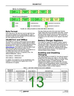
FIGURE 20. SMBus/ISL88731C READ AND WRITE PROTOCOL
The data (SDA) and clock (SCL) pins have Schmitt-
trigger inputs that can accommodate slow edges. Choose
pull-up resistors for SDA and SCL to achieve rise times
according to the SMBus specifications. The ISL88731C is
controlled by the data written to the registers described
in Table 1.
Byte Format
Every byte put on the SDA line must be eight bits long
and must be followed by an acknowledge bit. Data is
transferred with the most significant bit first (MSB) and
the least significant bit last (LSB).
ISL88731C and SMBus
Battery Charger Registers
The ISL88731C receives control inputs from the SMBus
interface. The serial interface complies with the SMBus
protocols as documented in the System Management Bus
Specification V1.1, which can be downloaded from
www.smbus.org. The ISL88731C uses the SMBus Read-
Word and Write-Word protocols (Figure 20) to
communicate with the smart battery. The ISL88731C is
an SMBus slave device and does not initiate
The ISL88731C supports five battery-charger registers
that use either Write-Word or Read-Word protocols, as
summarized in Table 1. ManufacturerID and DeviceID are
“read only” registers and can be used to identify the
ISL88731C. On the ISL88731C, ManufacturerID always
returns 0x0049 (ASCII code for “I” for Intersil) and
DeviceID always returns 0x0001.
communication on the bus. It responds to the 7-bit
address 0b0001001_ (0x12).
Enabling and Disabling
Charging
Read address = 0b00010011 and
Write address = 0b00010010.
After applying power to ISL88731C, the internal registers
contain their POR values (see Table 1). The POR values
for charge current and charge voltage are 0x0000. These
values disable charging. To enable charging, the
In addition, the ISL88731C has two identification (ID)
registers: a 16-bit device ID register and a 16-bit
manufacturer ID register.
ChargeCurrent register must be written with a number
>0x007F and the ChargeVoltage register must be written
with a number >0x000F. Charging can be disabled by
writing 0x0000 to either of these registers.
TABLE 1. BATTERY CHARGER REGISTER SUMMARY
REGISTER
ADDRESS
REGISTER NAME
ChargeCurrent
ChargeVoltage
InputCurrent
ManufacturerID
DeviceID
READ/WRITE
Read or Write
Read or Write
Read or Write
Read Only
DESCRIPTION
6-bit Charge Current Setting
11-bit Charge Voltage Setting
6-bit Charge Current Setting
Manufacturer ID
POR STATE
0x0000
0x14
0x15
0x3F
0xFE
0xFF
0x0000
0x0080
0x0049
Read Only
Device ID
0x0001
FN6978.0
March 8, 2010
13

 INTERSIL [ Intersil ]