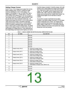
ISL88731
An adaptive gate drive scheme is used to control the dead
Theory of Operation
time between two switches. The dead time control circuit
monitors the LGATE output and prevents the upper side
MOSFET from turning on until 20ns after LGATE falls below
Introduction
The ISL88731 includes all of the functions necessary to
charge 1 to 4 cell Li-Ion and Li-polymer batteries. A high
efficiency synchronous buck converter is used to control the
charging voltage up to 19.2V and charging current up to 8A.
The ISL88731 also has input current limiting up to 11A. The
Input current limit, charge current limit and charge voltage
limit are set by internal registers written with SMBus. The
ISL88731 “Typical Application Circuit” is shown on Figure 2.
1V V , preventing cross-conduction and shoot-through.
GS
The same occurs for LGATE turn on. In order for the dead
time circuit to work properly, there must be a low resistance,
low inductance path from the LGATE driver to MOSFET
gate, and from the source of MOSFET to PGND. An internal
Schottky diode between the VDDP pin and BOOT pin keeps
the bootstrap capacitor charged.
The ISL88731 charges the battery with constant charge
current, set by the ChargeCurrent register, until the battery
voltage rises to a voltage set by the ChargeVoltage register.
The charger will then operate at a constant voltage. The
adapter current is monitored and if the adapter current rises to
the limit set by the InputCurrent register, battery charge
current is reduced so the charger does not reduce the adapter
current available to the system.
AC Adapter Detection
Connect the AC adapter voltage through a resistor divider to
ACIN to detect when AC power is available, as shown in
Figure 2. ACOK is an open-drain output and is active low
when ACIN is less than V
, and high when ACIN is
th,fall
above V
. The ACIN rising threshold is 3.2V (typ) with
th,rise
57mV hysteresis.
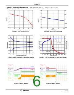
Current Measurement
The ISL88731 features a voltage regulation loop (VCOMP)
and 2 current regulation loops (ICOMP). The VCOMP
voltage regulation loop monitors VFB to limit the battery
charge voltage. The ICOMP current regulation loop limits the
battery charging current delivered to the battery to ensure
that it never exceeds the current set by the ChargeCurrent
register. The ICOMP current regulation loop also limits the
input current drawn from the AC adapter to ensure that it
never exceeds the limit set by the InputCurrent register, and
to prevent a system crash and AC adapter overload.
Use ICM to monitor the adapter current being sensed across
CSSP and CSSN. The output voltage range is 0 to 2.5V. The
voltage of ICM is proportional to the voltage drop across
CSSP and CSSN, and is given by Equation 1:
ICM = 20 ⋅ I
⋅ R
S1
INPUT
(EQ. 1)
where I
is the DC current drawn from the AC adapter.
adapter
It is recommended to have an RC filter at the ICM output for
minimizing the switching noise.
PWM Control
VDDP Regulator
The ISL88731 employs a fixed frequency PWM control
architecture with a feed-forward function. The feed-forward
function maintains a constant modulator gain of 11 to achieve
fast line regulation as the input voltage changes.
VDDP provides a 5.2V supply voltage from the internal LDO
regulator from DCIN and can deliver up to 30mA of
continuous current. The MOSFET drivers are powered by
VDDP. VDDP also supplies power to VCC through a low
pass filter as shown in the “TYPICAL APPLICATION
CIRCUIT” on page 2. Bypass VDDP and VCC with a 1µF
capacitor.
The duty cycle of the buck regulator is controlled by the lower
of the voltages on ICOMP and VCOMP. The voltage on
ICOMP and VCOMP are inputs to a Lower Voltage Buffer
(LVB) who’s output is the lower of the 2 inputs. The output of
the LVB is compared to an internal 400kHz ramp to produce
the Pulse Width Modulated signal that controls the UGATE
and LGATE drivers. An internal clamp holds the higher of the
2 voltages (0.3V) above the lower voltage. This speeds the
transition from voltage loop control to current loop control or
vice versa.
VDDSMB Supply
The VDDSMB input provides power to the SMBus interface.
Connect VDDSMB to VCC, or apply an external supply to
VDDSMB to keep the SMBus interface active while the
supply to DCIN is removed. When VDDSMB is biased the
internal registers are maintained. Bypass VDDSMB to GND
with a 0.1µF or greater ceramic capacitor.
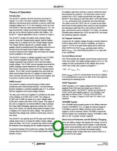
The ISL88731 can operate up to 99.6% duty cycle if the input
voltage drops close to or below the battery charge voltage
(drop out mode). The DC/DC converter has a timer to prevent
the frequency from dropping into the audible frequency range.
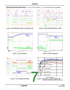
Short Circuit Protection and 0V Battery Charging
Since the battery charger will regulate the charge current to
the limit set by the ChargeCurrent register, it automatically
has short circuit protection and is able to provide the charge
current to wake up an extremely discharged battery.
Undervoltage trickle charge folds back current if there is a
short circuit on the output.
To prevent boosting of the system bus voltage, the battery
charger drives the lower FET in a way that prevents negative
inductor current.
FN9258.0
November 20, 2006
9

 INTERSIL [ Intersil ]