ISL88731
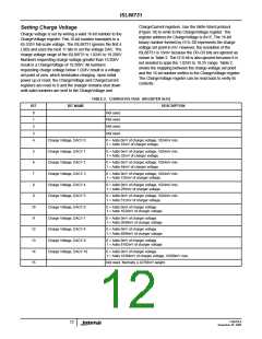
The STOP condition is a LOW to HIGH transition on the SDA
Undervoltage Detect and Battery Trickle Charging
line while SCL is HIGH. A STOP condition must be sent before
each START condition.
If the voltage at CSON falls below 2.5V ISL88731 reduces
the charge current limit to 128mA to trickle charge the
battery. When the voltage rises above 2.7V the charge
current reverts to the programmed value in the
ChargeCurrent register.
SDA
SCL
Over Temperature Protection
If the die temp exceeds +150°C, it stops charging. Once the
die temp drops below +125°C, charging will start up again.
S
P
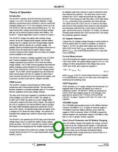
The System Management Bus
START
CONDITION
STOP
CONDITION
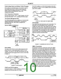
The System Management Bus (SMBus) is a 2 wire bus that
supports bidirectional communications. The protocol is
described briefly here. More detail is available from
www.smbus.org.
FIGURE 16. START AND STOP WAVEFORMS
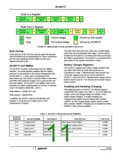
Acknowledge
Each address and data transmission uses 9 clock pulses. The
ninth pulse is the acknowledge bit (ACK). After the start
condition, the master sends 7 slave address bits and a R/W bit
during the next 8 clock pulses. During the ninth clock pulse, the
device that recognizes its own address holds the data line low
to acknowledge. The acknowledge bit is also used by both the
master and the slave to acknowledge receipt of register
addresses and data as described below.
General SMBus Architecture
VDDSMB
SMBus Slave
input
state
machine,
registers,
memory,
etc.
SCL
control
output
input
SMBus master
input
SDA
control
SCL
control
output
output
CPU
SCL
input
SDA
2
output
8
control
1
9
SMBus Slave
input
state
machine,
registers,
memory,
etc.
SCL
control
SDA
output
input
MSB
SDA
control
START
ACKNOWLEDGE
FROM SLAVE
output
2
FIGURE 17. ACKNOWLEDGE ON THE I C BUS
to other
slave devices
SMBus Transactions
Data Validity
All transactions start with a control byte sent from the SMBus
master device. The control byte begins with a Start condition,
followed by 7-bits of slave address (0001001 for the ISL88731)
followed by the R/W bit. The R/W bit is 0 for a write or 1 for a
read. If any slave devices on the SMBus bus recognize their
address, they will Acknowledge by pulling the serial data (SDA)
line low for the last clock cycle in the control byte. If no slaves
exist at that address or are not ready to communicate, the data
line will be 1, indicating a Not Acknowledge condition.
The data on the SDA line must be stable during the HIGH
period of the SCL, unless generating a START or STOP
condition. The HIGH or LOW state of the data line can only
change when the clock signal on the SCL line is LOW. Refer
to Figure 15.
SDA
Once the control byte is sent, and the ISL88731
acknowledges it, the 2nd byte sent by the master must be a
register address byte such as 0x14 for the ChargeCurrent
register. The register address byte tells the ISL88731 which
register the master will write or read. See Table 1 for details
of the registers. Once the ISL88731 receives a register
address byte it responds with an acknowledge.
SCL
DATA LINE CHANGE
STABLE
OF DATA
DATA VALID ALLOWED
FIGURE 15. DATA VALIDITY
START and STOP Conditions
As shown in Figure 16, START condition is a HIGH to LOW
transition of the SDA line while SCL is HIGH.
FN9258.0
November 20, 2006
10

 INTERSIL [ Intersil ]