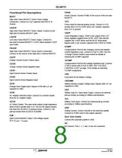
ISL88731
Absolute Maximum Ratings
Thermal Information
DCIN, CSSP, CSSN, CSOP, CSON, VFB . . . . . . . . . .-0.3V to +28V
CSSP-CSSN, CSOP-CSON, PGND-GND. . . . . . . . . -0.3V to +0.3V
PHASE to GND . . . . . . . . . . . . . . . . . . . . . . . . . . . . . . . -6V to +30V
BOOT to GND . . . . . . . . . . . . . . . . . . . . . . . . . . . . . . .-0.3V to +33V
BOOT to PHASE . . . . . . . . . . . . . . . . . . . . . . . . . . . . . .-0.3V to +6V
UGATE . . . . . . . . . . . . . . . . . . . . . . . . PHASE-0.3V to BOOT+0.3V
LGATE . . . . . . . . . . . . . . . . . . . . . . . . . PGND-0.3V to VDDP+0.3V
ICOMP, VCOMP, VREF, to GND . . . . . . . . . . . . -0.3V to VCC+0.3V
VDDSMB, SCL, SDA, ACIN, ACOK . . . . . . . . . . . . . . .-0.3V to +6V
VDDP, ICM, VCC to GND, VDDP to PGND. . . . . . . . . .-0.3V to +6V
Thermal Resistance (Typical, Notes 1, 2)
θ
(°C/W)
39
θ
(°C/W)
9.5
JA
JC
QFN Package. . . . . . . . . . . . . . . . . . . .
Junction Temperature Range. . . . . . . . . . . . . . . . . .-55°C to +150°C
Operating Temperature Range . . . . . . . . . . . . . . . .-10°C to +100°C
Storage Temperature . . . . . . . . . . . . . . . . . . . . . . . .-65°C to +150°C
Lead Temperature (Soldering, 10s) . . . . . . . . . . . . . . . . . . . . +300°C
CAUTION: Stress above those listed in “Absolute Maximum Ratings” may cause permanent damage to the device. This is a stress only rating and operation of the
device at these or any other conditions above those indicated in the operational section of this specification is not implied.
+150°C max junction temperature is intended for short periods of time to prevent shortening the lifetime. Operation close to +150°C junction may trigger the shutdown of
the device even before +150°C, since this number is specified as typical.
1. θ is measured with the component mounted on a highly effective thermal conductivity test board on free air. See Tech Brief TB379 for details.
JA
2. For θ , the “case temp” location is the center of the exposed metal pad on the package underside.
JC
Electrical Specifications DCIN = CSSP = CSSN = 18V, CSOP = CSON = 12V, VDDP = 5V, BOOT-PHASE = 5.0V, GND = PGND = 0V,
CVDDP = 1µF, IVDDP = 0mA, T = -10°C to +100°C
A
PARAMETER
CONDITIONS
MIN
TYP
16.8
MAX
UNITS
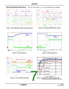
CHARGE VOLTAGE REGULATION
Battery Full Charge Voltage and Accuracy ChargeVoltage = 0x41A0
16.716
-0.5
16.884
0.5
V
%
V
ChargeVoltage = 0x3130
12.529
-0.5
12.592
8.4
12.655
0.5
%
V
ChargeVoltage = 0x20D0
8.350
-0.6
8.450
0.6
%
V
ChargeVoltage = 0x1060
4.163
-0.7
4.192
4.221
0.7
%
V
Battery Undervoltage Lockout Trip Point
for Trickle Charge
VFB rising
2.55
2.7
2.85
Battery Undervoltage Lockout Trip Point
Hysteresis
100
250
400
mV
mV
CHARGE CURRENT REGULATION
CSOP to CSON Full-Scale Current-Sense
Voltage
78.22
80.64
8.064
83.06
Charge Current and Accuracy
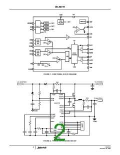
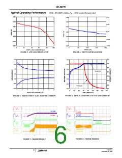
RS2 = 10mΩ (see Figure 2)
ChargingCurrent = 0x1f80
7.822
-3
8.306
3
A
%
RS2 = 10mΩ (see Figure 2)
ChargingCurrent = 0x0f80
3.809
-4
3.968
128
4.126
4
A
%
RS2 = 10mΩ (see Figure 2)
64
220
mA
ChargingCurrent = 0x0080
Charge Current Gain Error
Based on charge current = 128mA and 8.064A
-1.6
0
1.4
19
%
V
CSOP/CSON Input Voltage Range
FN9258.0
November 20, 2006
3

 INTERSIL [ Intersil ]