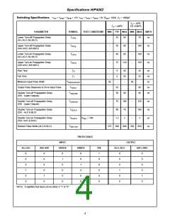
Specifications HIP4082
Absolute Maximum Ratings
Thermal Information
Supply Voltage, V . . . . . . . . . . . . . . . . . . . . . . . . . . . -0.3V to 16V Thermal Resistance, Junction-Ambient
θ
JA
DD
o
Logic I/O Voltages . . . . . . . . . . . . . . . . . . . . . . . -0.3V to V +0.3V
SOIC Package. . . . . . . . . . . . . . . . . . . . . . . . . . . . .
DIP Package . . . . . . . . . . . . . . . . . . . . . . . . . . . . . .
115 C/W
DD
o
o
o
Voltage on AHS, BHS. . . . . .-6V (Transient) to 80V (25 C to 150 C)
90 C/W
o
o
Voltage on AHS, BHS. . . . . -6V (Transient) to 70V (-55 C to150 C) Maximum Power Dissipation. . . . . . . . . . . . . . . . . . . . . . . . See Curve
o
o
Voltage on AHB, BHB. . . . . . . . . V
-0.3V to V
+V
Storage Temperature Range. . . . . . . . . . . . . . . . . .-65 C to +150 C
AHS, BHS
AHS, BHS
DD
o
Voltage on ALO, BLO . . . . . . . . . . . . . . . . . .V -0.3V to V +0.3V Operating Max. Junction Temperature . . . . . . . . . . . . . . . . . +150 C
SS
DD
o
Voltage on AHO, BHO . . . V
-0.3V to V
+0.3V Input
Lead Temperature (Soldering 10s) . . . . . . . . . . . . . . . . . . . . +300 C
AHS, BHS
AHB, BHB
Current, DEL . . . . . . . . . . . . . . . . . . . . . . . . . . . . . . . . -5mA to 0mA
Phase Slew Rate . . . . . . . . . . . . . . . . . . . . . . . . . . . . . . . . . . 20V/ns
(For SOIC - Lead Tips Only))
NOTE: All voltages are relative V unless otherwise specified.
SS
CAUTION: Stresses above those listed in “Absolute Maximum Ratings” may cause permanent damage to the device. This is a stress only rating and operation
of the device at these or any other conditions above those indicated in the operational sections of this specification is not implied.
Operating Conditions
Supply Voltage, V
. . . . . . . . . . . . . . . . . . . . . . . . . +8.5V to +15V Input Current, DEL . . . . . . . . . . . . . . . . . . . . . . . . . -4mA to -100µA
DD
Voltage on V . . . . . . . . . . . . . . . . . . . . . . . . . . . . . . -1.0V to +1.0V
SS
Voltage on AHB, BHB. . . . . . . . V
+7.5V to V
+V
AHS, BHS
AHS, BHS DD
Electrical Specifications
V
= V
= V
= 12V, V = V
= V
= 0V, R
= 100K
DD
AHB
BHB
SS
AHS
BHS
DEL
o
T = -55 C
J
o
o
T = +25 C
TO +150 C
J
PARAMETER
SYMBOL
TEST CONDITIONS
MIN TYP MAX MIN MAX UNITS
SUPPLY CURRENTS & UNDER VOLTAGE PROTECTION
V
Quiescent Current
I
All inputs = 0V, R
All inputs = 0V, R
= 100K
= 10K
1.2
2.2
1.5
2.5
0.5
65
.65
-
2.3 3.5 0.85
4
mA
mA
mA
mA
mA
µA
DD
DD
DEL
4.0
2.6
4.0
1.0
5.5
4.0
6.4
1.5
1.9
1.1
2.1
0.4
40
.45
-
6.0
4.2
6.6
1.6
250
2.0
-
DEL
V
Operating Current
I
f = 50kHz, no load
DD
DDO
50kHz, no load, R
AHI = BHI = 0V
= 10kΩ
DEL
AHB, BHB Off Quiescent Current
AHB, BHB On Quiescent Current
AHB, BHB Operating Current
AHS, BHS Leakage Current
I
, I
AHBL BHBL
I
, I
AHI = BHI = V
145 240
AHBH BHBH
DD
I
, I
f = 50kHz, CL = 1000pF
1.1
-
1.8
1.0
mA
µA
AHBO BHBO
I
V
= V
= V
= 80V
= 96
HLK
AHS
BHS
BHB
V
AHB
V
V
Rising Undervoltage Threshold
Falling Undervoltage Threshold
V
6.8
6.5
7.6 8.25 6.5
7.1
8.5
V
V
V
V
DD
DD
DDUV+
V
7.8 6.25 8.1
DDUV-
Undervoltage Hysteresis
AHB, BHB Undervoltage Threshold
INPUT PINS: ALI, BLI, AHI, BHI, & DIS
Low Level Input Voltage
High Level Input Voltage
Input Voltage Hysteresis
Low Level Input Current
High Level Input Current
TURN-ON DELAY PIN DEL
Dead Time
UVHYS
VHBUV
0.17 0.4 0.75 0.15 0.90
Referenced to AHS & BHS
5
6.0
7
4.5
7.5
0.8
-
V
Full Operating Conditions
Full Operating Conditions
-
2.5
-
-
-
1.0
-
2.7
-
V
V
IL
V
-
-
IH
35
mV
µA
µA
I
V
V
= 0V, Full Operating Conditions -145 -100 -60 -150 -50
IL
IN
IN
I
= 5V, Full Operating Conditions
-1
-
+1
-10 +10
IH
T
R
R
= 100K
= 10K
2.5
4.5
8.0
2.0
8.5
µS
µS
DEAD
DEL
DEL
0.27 0.5 0.75 0.2 0.85
GATE DRIVER OUTPUT PINS: ALO, BLO, AHO, & BHO
Low Level Output Voltage
High Level Output Voltage
Peak Pullup Current
V
I
I
= 50mA
= -50mA
= 0V
0.65
0.7
1.1
1.0
1.1
1.2
0.5
0.5
1.2
1.3
V
V
A
A
OL
OUT
V
-V
DD OH
OUT
I +
V
V
1.4
1.3
2.5 0.85 2.75
2.3 0.75 2.5
O
OUT
OUT
Peak Pulldown Current
I -
= 12V
O
3

 INTERSIL [ Intersil ]