HA-4741
Absolute Maximum Ratings
Thermal Information
o
o
o
T = 25 C Unless Otherwise Stated
A
Thermal Resistance (Typical, Note 2)
θ
( C/W)
θ
( C/W)
JA
JC
Supply Voltage Between V+ and V- Terminals. . . . . . . . . . . . . . 40V
Differential Input Voltage . . . . . . . . . . . . . . . . . . . . . . . . . . . . . . 30V
CERDIP Package. . . . . . . . . . . . . . . . .
PDIP Package . . . . . . . . . . . . . . . . . . .
SOIC Package . . . . . . . . . . . . . . . . . . .
Maximum Junction Temperature (Ceramic Package, Note 1). . . . .175 C
Maximum Junction Temperature (Plastic Packages, Note 1) . . . . .150 C
Maximum Storage Temperature Range. . . . . . . . . . -65 C to 150 C
Maximum Lead Temperature (Soldering 10s) . . . . . . . . . . . . 300 C
(SOIC - Lead Tips Only)
90
107
96
35
N/A
N/A
Input Voltage . . . . . . . . . . . . . . . . . . . . . . . . . . . . . . . . . . . V
SUPPLY
o
Output Short Circuit Duration (Note 3). . . . . . . . . . . . . . . . Indefinite
o
o
o
Operating Conditions
o
Temperature Range:
HA-4741-2 . . . . . . . . . . . . . . . . . . . . . . . . . . . . . . -55 C to 125 C
HA-4741-5 . . . . . . . . . . . . . . . . . . . . . . . . . . . . . . . . 0 C to 75 C
HA-4741-9 . . . . . . . . . . . . . . . . . . . . . . . . . . . . . . . -40 C to 85 C
o
o
o
o
o
o
CAUTION: Stresses above those listed in “Absolute Maximum Ratings” may cause permanent damage to the device. This is a stress only rating and operation of the
device at these or any other conditions above those indicated in the operational sections of this specification is not implied.
NOTES:
o
1. Maximum power dissipation, including output load, must be designed to maintain junction temperature below 175 C for the ceramic package,
o
and below 150 C for the plastic packages.
2. θ is measured with the component mounted on an evaluation PC board in free air.
JA
3. One amplifier may be shorted to ground indefinitely.
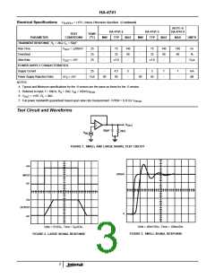
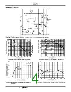
Electrical Specifications
V
= ±15V, Unless Otherwise Specified
SUPPLY
(NOTE 4)
HA-4741-2
HA-4741-5
TYP
HA-4741-9
TEST
CONDITIONS
TEMP.
( C)
o
PARAMETER
INPUT CHARACTERISTICS
Offset Voltage
MIN
TYP
MAX
MIN
MAX
MAX
UNITS
25
Full
Full
25
-
0.5
4
3
5
-
1
4
5
6.5
-
5
8.5
-
mV
mV
-
-
o
Average Offset Voltage Drift
Bias Current
-
5
-
-
5
µV/ C
-
60
-
200
325
30
75
-
-
60
-
300
400
50
100
-
300
400
50
100
-
nA
nA
Full
25
-
-
Offset Current
-
15
-
-
30
-
nA
Full
Full
25
-
-
nA
Common Mode Range
±12
-
±12
-
V
Differential Input Resistance
Input Voltage Noise
-
-
0.5
9
-
-
-
0.5
9
-
-
MΩ
nV/√Hz
f = 1kHz
25
-
-
-
TRANSFER CHARACTERISTICS
Large Signal Voltage Gain
V
= ±10V,
25
Full
25
50
25
80
74
66
2.5
100
-
-
-
-
-
-
-
25
15
80
74
66
2.5
50
-
-
-
-
-
-
-
-
-
-
-
-
-
kV/V
kV/V
dB
OUT
R = 2kΩ
L
Common Mode Rejection Ratio
95
-
95
-
Full
25
dB
Channel Separation (Note 5)
Small Signal Bandwidth
OUTPUT CHARACTERISTICS
Output Voltage Swing
69
3.5
69
3.5
dB
25
MHz
R = 10kΩ
Full
Full
25
±12
±10
-
±13.7
±12.5
25
-
-
-
-
-
±12
±10
-
±13.7
±12.5
25
-
-
-
-
-
-
-
-
-
-
V
V
L
Output Voltage Swing
R = 2kΩ
L
Full Power Bandwidth (Notes 6, 7)
Output Current
kHz
mA
Ω
V
= ±10V
Full
25
±5
-
±15
±5
-
±15
OUT
Output Resistance
300
300
2

 INTERSIL [ Intersil ]