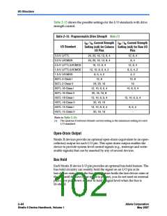
I/O Structure
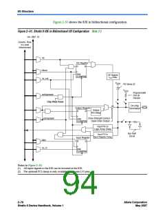
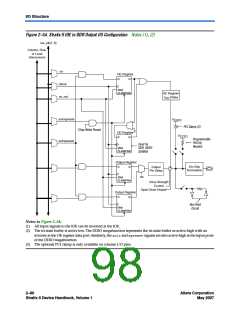
Figure 2–54. Stratix II IOE in DDR Output I/O Configuration Notes (1), (2)
ioe_clk[7..0]
Column, Row,
or Local
Interconnect
oe
OE Register
D
Q
clkout
ENA
CLRN/PRN
OE Register
Delay
ce_out
t
CO
aclr/apreset
sclr/spreset
V
CCIO
PCI Clamp (3)
Chip-Wide Reset
OE Register
V
CCIO
D
Q
Programmable
Pull-Up
Resistor
Used for
DDR, DDR2
SDRAM
ENA
CLRN/PRN
Output Register
D
Q
On-Chip
Termination
Output
Pin Delay
clk
ENA
CLRN/PRN
Drive Strength
Control
Open-Drain Output
Output Register
D
Q
Bus-Hold
Circuit
ENA
CLRN/PRN
Notes to Figure 2–54:
(1) All input signals to the IOE can be inverted at the IOE.
(2) The tri-state buffer is active low. The DDIO megafunction represents the tri-state buffer as active-high with an
inverter at the OE register data port. Similarly, the aclrand apresetsignals are also active-high at the input ports
of the DDIO megafunction.
(3) The optional PCI clamp is only available on column I/O pins.
2–80
Altera Corporation
May 2007
Stratix II Device Handbook, Volume 1

 INTEL [ INTEL ]