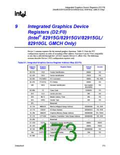
Host-PCI Express* Bridge Registers (D1:F0)
(Intel® 82915G/82915P/82915PL Only)
R
8.1.58
LE1A—Link Entry 1 Address (D1:F0)
PCI Device:
Address Offset:
Default Value:
Access:
1
158h
0000000000000000h
R/WO
Size:
64 bits
This register provides the second part of a Link Entry that declares an internal link to another
Root Complex Element.
Bit
Access &
Default
Description
63:32
31:12
Reserved
R/WO
Link Address: This field indicates memory-mapped base address of the RCRB
0 0000h
that is the target element (Egress Port) for this link entry.
11:0
Reserved
8.1.59
PEGSSTS—PCI Express*-G Sequence Status (D1:F0)
PCI Device:
Address Offset:
Default Value:
Access:
1
218h
0000000000000FFFh
RO
Size:
64 bits
This register provides PCI Express status reporting that is required by the PCI Express
specification.
Bit
Access &
Default
Description
63:60
59:48
Reserved
RO
000h
Next Transmit Sequence Number: Value of the NXT_TRANS_SEQ counter.
This counter represents the transmit Sequence number to be applied to the next
TLP to be transmitted onto the Link for the first time.
47:44
43:32
Reserved
RO
Next Packet Sequence Number: Packet sequence number to be applied to the
000h
next TLP to be transmitted or re-transmitted onto the Link.
31:28
27:16
Reserved
RO
Next Receive Sequence Number: This is the sequence number associated with
000h
the TLP that is expected to be received next.
15:12
11:0
Reserved
RO
Last Acknowledged Sequence Number: This is the sequence number
FFFh
associated with the last acknowledged TLP.
§
Datasheet
171

 INTEL [ INTEL ]