LIST OF FIGURES
PAGE
Figure 1
Figure 2
Figure 3
Figure 4
Figure 5
Figure 6
Figure 7
Figure 8
Figure 9
Figure 10
Figure 11
Figure 12
Figure 13
Figure 14
Figure 15
Figure 16
Figure 17
Figure 18
Figure 19
Figure 20
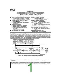
The 80960SB Processor’s Highly Parallel Architecture ................................................................0
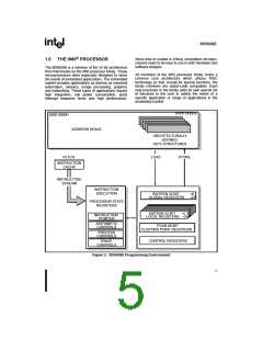
80960SB Programming Environment ...........................................................................................1
Instruction Formats ......................................................................................................................4
Multiple Register Sets Are Stored On-Chip ..................................................................................6
Connection Recommendation for LOCK .................................................................................... 11
Typical Supply Current vs. Case Temperature ........................................................................... 12
Typical Current vs. Frequency (Room Temp) ............................................................................. 12
Typical Current vs. Frequency (Hot Temp) ................................................................................. 13
Capacitive Derating Curve ......................................................................................................... 13
Test Load Circuit for Three-State Output Pins ............................................................................ 13
Drive Levels and Timing Relationships for 80960SB Signals ..................................................... 15
Processor Clock Pulse (CLK2) ................................................................................................... 18
RESET Signal Timing ................................................................................................................. 18
HOLD Timing .............................................................................................................................. 19
80-Lead EIAJ Quad Flat Pack (QFP) Package .......................................................................... 20
84-Lead Plastic Leaded Chip Carrier (PLCC) Package ............................................................. 21
Non-Burst Read and Write Transactions Without Wait States .................................................... 27
Quad Word Burst Read Transaction With 1, 0, 0, 0, 0, 0, 0, 0 Wait States ................................ 28
Burst Write Transaction With 2, 1, 1, 1 Wait States (6-8 Bytes Transferred) .............................. 29
Accesses Generated by Quad Word Read Bus Request,
Misaligned One Byte from Quad Word Boundary 1, 0, 0, 0, 0, 0, 0, 0 Wait States
30
Figure 21
Figure 22
Interrupt Acknowledge Cycle ...................................................................................................... 31
Cold Reset Waveform ................................................................................................................ 32
LIST OF TABLES
Table 1
Table 2
Table 3
Table 4
Table 5
Table 6
Table 7
Table 8
Table 9
Table 10
Table 11
Table 12
Table 13
Table 14
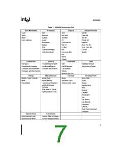
80960SB Instruction Set ..............................................................................................................3
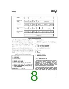
Memory Addressing Modes .........................................................................................................4
Sample Floating-Point Execution Times (µs) at 16 MHz ..............................................................6
80960SB Pin Description: Bus Signals ........................................................................................8
80960SB Pin Description: Support Signals ................................................................................ 10
DC Characteristics ..................................................................................................................... 14
80960SB AC Characteristics (10 MHz) ...................................................................................... 16
80960SB AC Characteristics (16 MHz) ...................................................................................... 17
80960SB QFP Pinout — In Pin Order ........................................................................................ 22
80960SB QFP Pinout — In Signal Order ................................................................................... 23
80960SB PLCC Pinout — In Pin Order ...................................................................................... 24
80960SB PLCC Pinout — In Signal Order ................................................................................. 25
80960SB QFP Package Thermal Characteristics ...................................................................... 26
80960SB PLCC Package Thermal Characteristics .................................................................... 26
iii

 INTEL [ INTEL ]