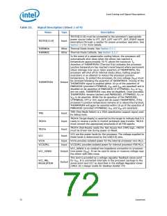
Land Listing and Signal Descriptions
Table 25.
Signal Description (Sheet 1 of 9)
Name
Type
Description
TESTHI[13:0] must be connected to the processor’s appropriate
power source (refer to VTT_OUT_LEFT and VTT_OUT_RIGHT signal
description) through a resistor for proper processor operation. See
Section 2.4 for more details.
TESTHI[13:0]
Input
THERMDA
THERMDC
Other Thermal Diode Anode. See Section 5.2.7.
Other Thermal Diode Cathode. See Section 5.2.7.
In the event of a catastrophic cooling failure, the processor will
automatically shut down when the silicon has reached a
temperature approximately 20 °C above the maximum TC.
Assertion of THERMTRIP# (Thermal Trip) indicates the processor
junction temperature has reached a level beyond where permanent
silicon damage may occur. Upon assertion of THERMTRIP#, the
processor will shut off its internal clocks (thus, halting program
execution) in an attempt to reduce the processor junction
temperature. To protect the processor, its core voltage (VCC) must
be removed following the assertion of THERMTRIP#. Driving of the
THERMTRIP# signal is enabled within 10 µs of the assertion of
THERMTRIP#
Output
PWRGOOD (provided VTTPWRGD, VTT, and VCC are asserted) and is
disabled on de-assertion of PWRGOOD (if VTTPWRGD, VTT, or VCC
are not valid, THERMTRIP# may also be disabled). Once activated,
THERMTRIP# remains latched until PWRGOOD, VTTPWRGD, VTT or
V
CC is de-asserted. While the de-assertion of the PWRGOOD,
VTTPWRGD, VTT or VCC signal will de-assert THERMTRIP#, if the
processor’s junction temperature remains at or above the trip level,
THERMTRIP# will again be asserted within 10 µs of the assertion of
PWRGOOD (provided VTTPWRGD, VTT, and VCC are asserted).
TMS (Test Mode Select) is a JTAG specification support signal used
by debug tools.
TMS
Input
Input
TRDY# (Target Ready) is asserted by the target to indicate that it is
ready to receive a write or implicit writeback data transfer. TRDY#
must connect the appropriate pins/lands of all FSB agents.
TRDY#
TRST# (Test Reset) resets the Test Access Port (TAP) logic. TRST#
must be driven low during power on Reset.
TRST#
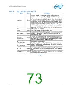
VCC
Input
Input
VCC are the power lands for the processor. The voltage supplied to
these lands is determined by the VID[5:0] pins.
VCCA
Input
Input
VCCA provides isolated power for the internal processor core PLLs.
VCCIOPLL provides isolated power for internal processor FSB PLLs.
VCC_SENSE is an isolated low impedance connection to processor
VCCIOPLL
VCC_SENSE
Output core power (VCC). It can be used to sense or measure voltage near
the silicon with little noise.
This land is provided as a voltage regulator feedback sense point
VCC_MB_
REGULATION
for VCC. It is connected internally in the processor package to the
sense point land U27 as described in the Voltage Regulator-Down
Output
(VRD) 10.1 Design Guide for Desktop Socket 775.
72
Datasheet

 INTEL [ INTEL ]