Processor Configuration Registers
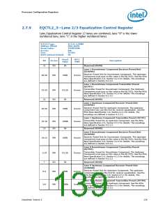
2.7.10
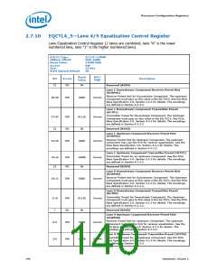
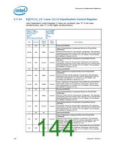
EQCTL4_5—Lane 4/5 Equalization Control Register
Lane Equalization Control Register (2 lanes are combined, lane "0" is the lower
numbered lane, lane "1" is the higher numbered lane).
B/D/F/Type:
Address Offset:
Reset Value:
Access:
0/1/0–1/MMR
DA8–DABh
07080708h
RW
Size:
32 bits
BIOS Optimal Default
0h
Reset
Value
RST/
PWR
Bit
Access
Description
31
RO
0h
Reserved (RSVD)
Lane 1 Downstream Component Receiver Preset Hint
(DCRPH1)
Receiver Preset Hint for Downstream Component. The Upstream
Component must pass on this value in the EQ TS2’s. See the PCIe
Base Specification 3.0, Section 4.2.3 for details. The encodings
are defined in Section 4.2.3.2.
30:28
RW
000b
Uncore
Uncore
Lane 1 Downstream Component Transmitter Preset
(DCTP1)
Transmitter Preset for Downstream Component. The Upstream
Component must pass on this value in the EQ TS2’s. See PCIe
Base Specification 3.0, Section 4.2.3 for details. The encodings
are defined in Section 4.2.3.2.
27:24
23
RW
RO
RW
0111b
0h
Reserved (RSVD)
Lane 1 Upstream Component Receiver Preset Hint
(UCRPH1)
Receiver Preset Hint for Upstream Component. The upstream
component may use this hint for receiver equalization. See the
PCIe Base Specification 3.0, Section 4.2.3 for details. The
encodings are defined in Section 4.2.3.2.
22:20
000b
Uncore
Uncore
Lane 1 Upstream Component Transmitter Preset (UCTP1)
Transmitter Preset for an Upstream Component. See the PCIe
Base Specification 3.0, Section 4.2.3 for details. The encodings
are defined in Section 4.2.3.2.
19:16
15
RW
RO
1000b
0h
Reserved (RSVD)
Lane 0 Downstream Component Receiver Preset Hint
(DCRPH0)
Receiver Preset Hint for Downstream Component. The Upstream
Component must pass on this value in the EQ TS2’s. See the PCIe
Base Specification 3.0, Section 4.2.3 for details. The encodings
are defined in Section 4.2.3.2.
14:12
RW
000b
Uncore
Uncore
Lane 0 Downstream Component Transmitter Preset
(DCTP0)
Transmitter Preset for Downstream Component. The Upstream
Component must pass on this value in the EQ TS2’s. See the PCIe
Base Specification 3.0, Section 4.2.3 for details. The encodings
are defined in Section 4.2.3.2.
11:8
7
RW
RO
RW
0111b
0h
Reserved (RSVD)
Lane 0 Upstream Component Receiver Preset Hint
(UCRPH0)
Receiver Preset Hint for Upstream Component. The upstream
component may use this hint for receiver equalization. See the
PCIe Base Specification 3.0, Section 4.2.3 for details. The
encodings are defined in Section 4.2.3.2.
6:4
000b
Uncore
Uncore
Lane 0 Upstream Component Transmitter Preset (UCTP0)
Transmitter Preset for an Upstream Component. See the PCIe
Base Specification 3.0, Section 4.2.3 for details. The encodings
are defined in Section 4.2.3.2.
3:0
RW
1000b
140
Datasheet, Volume 2

 INTEL [ INTEL ]