Electrical Characteristics
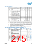
Table 8-22. Power Management Timings (Sheet 3 of 3)
Sym
Parameter
Min
Max
Units
Notes
Fig
LAN Power Rails active to LAN_RST#
deassertion
t305a
1
ms
18
LAN_RST# assertion to LAN Power Rails
inactive
t305b
t306
t307
20
0
ns
ms
us
25
24
LANRST# assertion to PWROK assertion
SLP_S3# active to Vcc supplies inactive
(nominal voltage -5%)
5
8-17
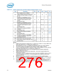
RSMRST# deassertion to CLPWROK
assertion
t308a
0
ms
Controller Link Power Rails active to
CLPWROK assertion
t308b
t308c
1
0
ms
ms
CLPWROK assertion to PWROK assertion
Other Timings
THRMTRIP# active to SLP_S3#, SLP_S4#,
SLP_S5# active
t310
t311
175
50
ns
RSMRST# rising edge transition from 20%
to 80%
μs
t312
t313
RSMRST# falling edge transition
SLP_M# active to RSMRST# active
21
500
μs
NOTES:
1.
These transitions are clocked off the internal RTC. 1 RTC clock is approximately from
28.992 µs to 32.044 µs.
2.
The ICH10 STPCLK# assertion will trigger the processor to send a stop grant acknowledge
cycle. The timing for this cycle getting to the ICH10 is dependant on the processor and the
memory controller.
3.
4.
These transitions are clocked off the 33 MHz PCICLK. 1 PCICLK is approximately 30 ns.
The ICH10 has no maximum timing requirement for this transition. It is up to the system
designer to determine if the SLP_S3#, SLP_S4# and SLP_S5# signals are used to control
the power planes.
5.
6.
If the transition to S5 is due to Power Button Override, SLP_S3#, SLP_S4# and SLP_S5#
are asserted together similar to timing t287 (PCIRST# active to SLP_S3# active).
If there is no RTC battery in the system, so VccRTC and the VccSus supplies come up
together, the delay from RTCRST# and RSMRST# inactive to SUSCLK toggling may be as
much as 2.5 s.
7.
8.
This value is programmable in multiples of 1024 PCI CLKs. Maximum is 8192 PCI CLKs
(245.6 µs).
The Min/Max times depend on the programming of the “SLP_S4# Minimum Assertion
Width” and the “SLP_S4# Assertion Stretch Enable bits (D31:F0:A4h bits 5:3)”.
Note that this does not apply for synchronous SMIs.
9.
10.
11.
This is a clock generator specification
If the (G)MCH does not have the CPUSLP# signal, then the minimum value can be
16 PCICLK.
12.
13.
This is non-zero to enforce the minimum assert time for DPRSLPVR. If the minimum assert
time for DPRSLPVR has been met, then this is permitted to be 0.
This is non-zero to enforce the minimum assert time for STP_CPU#. If the minimum assert
time for STP_CPU# has been met, then this is permitted to be 0.
This value should be at most a few clocks greater than the minimum.
When Intel AMT enabled, S4_STATE# indicates if system is in S4 state or below.
For t234 and t298, the SLP_M# stretching logic can push the Max value much larger than
the Min (e.g., up to 3 seconds). With the installation of the Intel Manageability Engine
14.
15.
16.
Datasheet
279

 INTEL [ INTEL ]