System Address Map
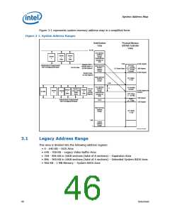
3 System Address Map
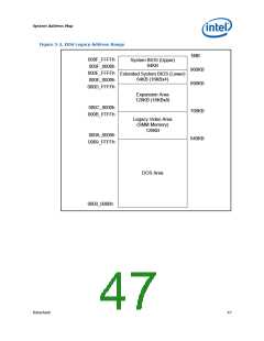
The 82G35 GMCH supports 64GB or 4 GB of addressable memory space and 64 KB+3
of addressable I/O space. There is a programmable memory address space under the
1 MB region which is divided into regions which can be individually controlled with
programmable attributes such as Disable, Read/Write, Write Only, or Read Only.
Attribute programming is described in the Register Description section. This section
focuses on how the memory space is partitioned and what the separate memory
regions are used for. I/O address space has simpler mapping and is explained near
the end of this section.
The HREQ[4:3] FSB pins are decoded to determine whether the access is 32 bit or 36
bit.
The G35 GMCH supports a maximum of 8GB of DRAM, no DRAM memory will be
accessible above 8 GB. DRAM capacity is limited by the number of address pins
available. There is no hardware lock to stop someone from inserting more memory
than is addressable.
In the following sections, it is assumed that all of the compatibility memory ranges
reside on the DMI Interface. The exception to this rule is VGA ranges, which may be
mapped to PCI Express*, DMI, or to the internal graphics device (IGD). In the
absence of more specific references, cycle descriptions referencing PCI should be
interpreted as the DMI Interface/PCI, while cycle descriptions referencing PCI Express
or IGD are related to the PCI Express bus or the internal graphics device respectively.
The reclaim base/reclaim limit registers remap logical accesses bound for addresses
above 4G onto physical addresses that fall within DRAM.
The Address Map includes a number of programmable ranges:
•
⎯
Device 0
PXPEPBAR – Egress port registers. Necessary for setting up VC1 as an
isochronous channel using time based weighted round robin arbitration. (4 KB
window)
MCHBAR – Memory mapped range for internal GMCH registers. For example,
memory buffer register controls. (16 KB window)
PCIEXBAR – Flat memory-mapped address spaced to access device
configuration registers. This mechanism can be used to access PCI configuration
space (0-FFh) and Extended configuration space (100h–FFFh) for PCI Express
devices.
⎯
⎯
⎯
⎯
DMIBAR –This window is used to access registers associated with the
GMCH/ICH Serial Interconnect (DMI) register memory range. (4 KB window)
GGC – GMCH graphics control register. Used to select the amount of main
memory that is pre-allocated to support the internal graphics device in VGA (non-
linear) and Native (linear) modes. (0–64 MB options).
•
⎯
Device 1
MBASE1/MLIMIT1 – PCI Express port non-prefetchable memory access
window.
⎯
⎯
PMUBASE1/PMULIMIT1 – PCI Express port prefetchable memory access
window.
IOBASE1/IOLIMIT1 – PCI Express port IO access window.
44
Datasheet

 INTEL [ INTEL ]