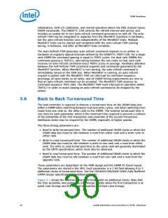
DDR Interface
3.8.3
Automatic DDR Bus Calibration
The AMB has two automatic DDR bus calibration functions that must be executed
before read data can be captured reliably. These functions issue a series of write and
read transactions on the DRAM bus, analyze the read data captured, and program a set
of calibration results configuration registers. During subsequent operations, these
configuration registers control the DDR I/O circuits and ensure proper data capture.
DIMM memory contents are not preserved during calibration. Calibration can take up to
several ms to complete. The following steps run the calibration:
1. Program the DCALCSR to 0x8000000C. This selects and initiates the first of two
calibrations.
2. Poll the DCALCSR until bit 31 is cleared to zero by hardware.
3. Program the DCALCSR to 0x80000005. This selects/initiates the second calibration.
4. Poll the DCALCSR until bit 31 is cleared to zero by hardware.
3.8.4
Receive Enable Calibration
The DQS input receiver needs to be disabled when the DDR bus is floating (tri-stated),
for example, between the read and write data transfers. Otherwise, the floating strobe
would cause spurious data to be written into the read data FIFO. Also, the DQS input
receiver needs to be disabled during a write so that the write data strobes do not cause
unwanted data or check-bits to be written into the read data FIFO.
During a read, the DRAM’s initially drive the DQS signals low for a full cycle. This is the
preamble. After the preamble, the DQS signals are toggled twice per cycle, for every
cycle there is a data transfer, which is determined by the configured burst length and
the number of back-to-back read commands that were issued to the selected rank.
After the last DQS falling edge, the DQS signal is driven low for a half cycle. This is the
post-amble. After the post-amble the DQS signals are tri-stated.
The AMB automatically finds the end of the preamble of each of the 18 DQS pairs on
the DDR bus. That is, it finds the location of the first waveform transition that defines
the end of the preamble of each DQS pair. Once this is complete, the AMB calculates
the location of the center of the preambles, and stores this information for use during
read transactions. Receiver calibration is initiated by setting the DCALCSR.START CSR.
Hardware clears this bit when the calibration is complete. The calibration method
modifies the data contents of the DIMM.
3.8.5
DQS Delay Calibration
The DQS Delay calibration adjusts the AMB Component’s on-chip delay circuits that
align DQS signals to the center of their associated DQ/CB data eyes at the capture flops
in the DDR I/O cluster. This maximizes the DQ/CB setup and hold time at these flops,
which capture source synchronous data from the DDR data bus.
DQS delay calibration is initiated by setting the DCALCSR.START CSR. Hardware clears
this bit when the calibration is complete. The calibration method modifies the data
contents of the DIMM. The calibration is accomplished by issuing a series of write and
read transactions, and comparing expected to captured data
34
Intel® 6400/6402 Advanced Memory Buffer Datasheet

 INTEL [ INTEL ]