DDR Interface
3.7.1
S3 Recovery Configuration Registers
The following CSRs should be stored in non-volatile memory before entering S3 mode
and restored before normal DRAM transactions begin.
• DRC
• MTR
• DSREFTC
• DAREFTC
• DDR2ODTC
• CMD2DATANXT
• S3RESTORE[15:0]
• PERSBYTE[13:0] - SPD Personality Bytes
3.8
DDR Calibration
The following sections describe these DDR calibration and initialization features:
• DRAM initialization and (E)MRS command CSR’s and FSM
• DQS failure CSR
• DQS receive enable calibration
• DQS calibration
3.8.1
DRAM Initialization and (E)MRS FSM
The AMB provides a set of CSR’s and an FSM that allow BIOS to manage DRAM power
up initialization and set DRAM mode register bits. All commands needed for DRAM
initialization can be generated, including precharge, refresh, mode register set (MRS),
and extended mode register set EMRS commands. A self-refresh command can also be
generated, although this is not required for initialization. The initialization/(E)MRS FSM
only controls the issuing of single commands, and does not automatically initialize the
DRAM. It is the responsibility of software to control the command sequence to correctly
initialize the DRAM.
The set of CSR’s include the DCALCSR and DCALADDR registers. The fields of these
CSR’s are described in detail in the configuration register chapter.
The DCALCSR is used to select the command to be issued, which ranks to select, start
the FSM that issues the command, and provide completion status.
The DCALADDR sets the bank and address issued to the DRAM, and therefore defines
the type of (E)MRS to be issued, including limited OCD commands. The DCALADDR can
also be used to configure a precharge command as a “precharge all” command.
DCALADDR[31:16] defines the DDR address bus during these commands, and
DCALADDR[2:0] defines the ddr bank address bus.
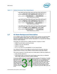
The FSM that controls this function can have as few as three states: idle, issue
command, and clear start bit. When the DCALCSR.START bit is set, and the
DCALCSR.OPCODE bits select one of the command options, the FSM transitions from
idle to the “issue command” state. After the command is issued, the FSM clears the
DCALCSR.START bit and returns to the idle state. A more elaborate FSM may also be
implemented. Firmware is required to control the minimum command spacing to meet
all DRAM timing requirements. After setting the start bit, firmware should poll the
32
Intel® 6400/6402 Advanced Memory Buffer Datasheet

 INTEL [ INTEL ]