Registers
Device:
NodeID
Function: 1
Offset:
98h
Bit
Attr
Default
Description
9:8
RWST
0h
size:
00 = one byte
01 = two bytes
10 = three bytes
11 = four bytes
Note: This field only defined for errors on Config Register Writes. This
field is undefined for other transactions.
7:0
RWST
0h
register address:
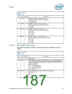
14.3.3.5
RECFBD[9:0]: FBD Error Log
.This register contains FBD frame data received that matches the logged frame error.
Captures {BC} from frame N and A from frame N+1 where
[11:8] = A[n+1]
[7:4] = C[n] slot
[3:0] = B[n] slot
The contents of this register are only valid when one of the errors that set this register
is logged in the FERR register. The contents of this register should not change until the
error indication is cleared from the FERR register.
Device:
NodeID
Function: 1
Offset:
Bit
AEh, ACh, AAh, A8h, A6h, A4h, A2h, A0h, 9Eh, 9Ch
Attr
Default
Description
15:12
11:0
RV
0
0
Reserved
FRMDATA: Frame data for lane n
RWST
14.3.4
PERSONALITY BYTES Loaded From the SPD
These bytes allow for AMB implementation specific settings to be loaded in an
architected way by BIOS without BIOS being aware of specific AMB requirements. Each
AMB vendor defines how these bytes should be loaded for the specific DIMM being built.
The values to be loaded into these bytes are stored in the SPD EEPROM on the DIMM.
The first six bytes are required to be loaded into the AMB via SMBus before link
initialization to allow for configuration information needed for robust link operation.
The remaining 8 bytes must be loaded before the FBD begins normal operation.
Usage of these bytes can include
• DDR electrical parameters to optimize performance on a given DIMM
— For example, DLL delay settings, various I/O driver slew settings,
• Enable/disable of various optimizations that may have been included in the design
but can be turned off if they are not needed on this DIMM or they have
unanticipated side effects - for example, power save modes, alternate clock
recovery algorithms, and so forth.
• Temperature Sensor offsets
Intel® 6400/6402 Advanced Memory Buffer Datasheet
183

 INTEL [ INTEL ]