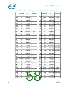
Land Listing and Signal Descriptions
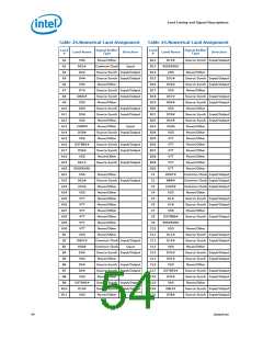
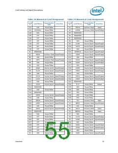
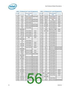
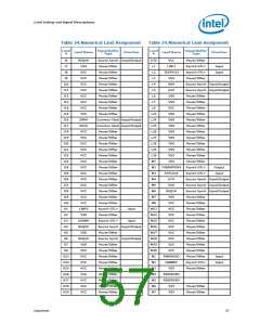
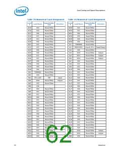
Table 24.Numerical Land Assignment
Table 24.Numerical Land Assignment
Land
#
Signal Buffer
Type
Land
#
Signal Buffer
Type
Land Name
Direction
Land Name
Direction
N8
N23
N24
N25
N26
N27
N28
N29
N30
P1
VCC
VCC
Power/Other
Power/Other
Power/Other
Power/Other
Power/Other
Power/Other
Power/Other
Power/Other
Power/Other
Power/Other
Asynch GTL+
Asynch GTL+
Power/Other
R30
T1
VSS
COMP1
COMP5
VSS
Power/Other
Power/Other
Power/Other
Power/Other
Input
Input
VCC
T2
VCC
T3
VCC
T4
A11#
A9#
Source Synch Input/Output
Source Synch Input/Output
Power/Other
VCC
T5
VCC
T6
VSS
VCC
T7
VSS
Power/Other
VCC
T8
VCC
Power/Other
TESTHI11
SMI#
INIT#
VSS
Input
Input
Input
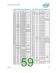
T23
T24
T25
T26
T27
T28
T29
T30
U1
VCC
Power/Other
P2
VCC
Power/Other
P3
VCC
Power/Other
P4
VCC
Power/Other
P5
RESERVED
A4#
VCC
Power/Other
P6
Source Synch Input/Output
Power/Other
VCC
Power/Other
P7
VSS
VCC
Power/Other
P8
VCC
Power/Other
VCC
Power/Other
P23
P24
P25
P26
P27
P28
P29
P30
R1
VSS
Power/Other
VSS
Power/Other
VSS
Power/Other
U2
AP0#
AP1#
A13#
A12#
A10#
VSS
Common Clock Input/Output
Common Clock Input/Output
Source Synch Input/Output
Source Synch Input/Output
Source Synch Input/Output
Power/Other
VSS
Power/Other
U3
VSS
Power/Other
U4
VSS
Power/Other
U5
VSS
Power/Other
U6
VSS
Power/Other
U7
VSS
Power/Other
U8
VCC
Power/Other
FC2
Power/Other
Power/Other
Asynch GTL+
Input
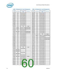
U23
U24
U25
U26
U27
U28
U29
U30
V1
VCC
Power/Other
R2
VSS
VCC
Power/Other
R3
FERR#/PBE#
A8#
Output
VCC
Power/Other
R4
Source Synch Input/Output
Power/Other
VCC
Power/Other
R5
VSS
VCC
Power/Other
R6
ADSTB0#
VSS
Source Synch Input/Output
Power/Other
VCC
Power/Other
R7
VCC
Power/Other
R8
VCC
Power/Other
VCC
Power/Other
R23
R24
R25
R26
R27
R28
R29
VSS
Power/Other
MSID1
LL_ID0
VSS
Power/Other
Power/Other
Power/Other
Output
Output
VSS
Power/Other
V2
VSS
Power/Other
V3
VSS
Power/Other
V4
A15#
A14#
VSS
Source Synch Input/Output
Source Synch Input/Output
Power/Other
VSS
Power/Other
V5
VSS
Power/Other
V6
VSS
Power/Other
V7
VSS
Power/Other
58
Datasheet

 INTEL [ INTEL ]