IN74HCT373A
AC ELECTRICAL CHARACTERISTICS
±
(VCC =5.0 V 10%, CL=50pF,Input tr=tf=6.0 ns)
Guaranteed Limit
Symbol
Parameter
Unit
25 °C
to
≤85°C
≤125°C
-55°C
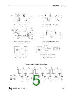
tPLH, tPHL Maximum Propagation Delay, Input D to Q
(Figures 1 and 5)
28
32
30
35
12
35
40
38
44
15
42
48
45
53
18
ns
ns
ns
ns
ns
tPLH, tPHL Maximum Propagation Delay , Latch Enable to Q
(Figures 2 and 5)
tPLZ, tPHZ Maximum Propagation Delay ,Output Enable to Q
(Figures 3 and 6)
tPZL, tPZH Maximum Propagation Delay , Output Enable to
Q (Figures 3 and 6)
tTLH, tTHL Maximum Output Transition Time, Any Output
(Figures 1 and 5)
CIN
Maximum Input Capacitance
10
15
10
15
10
15
pF
pF
COUT
Maximum Three-State Output Capacitance
(Output in High-Impedance State)
Power Dissipation Capacitance (Per Latch)
Typical @25°C,VCC=5.0 V
CPD
Used to determine the no-load dynamic power
consumption:
65
pF
PD=CPDVCC2f+ICCVCC
TIMING REQUIREMENTS
±
(VCC =5.0 V 10%, CL=50pF,Input tr=tf=6.0 ns)
Guaranteed Limit
Symbol
tSU
Parameter
Unit
ns
25 °C to
-55°C
≤85°C
≤125°C
Minimum Setup Time, Input D
to Latch Enable
10
13
15
(Figure 4)
th
Minimum Hold Time,Latch
Enable to Input D
(Figure 4)
10
13
15
ns
tw
Minimum Pulse Width, Latch
Enable (Figure 2)
12
15
18
ns
ns
tr, tf
Maximum Input Rise and Fall
Times (Figure 1)
500
500
500
374

 INTEGRAL [ INTEGRAL CORP. ]