XMC4500
XMC4000 Family
General Device Information
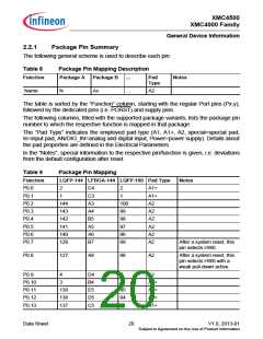
2.2.1
Package Pin Summary
The following general scheme is used to describe each pin:
Table 8
Function
Package Pin Mapping Description
Package A
Package B
...
Pad
Notes
Type
Name
N
Ax
...
A2
The table is sorted by the “Function” column, starting with the regular Port pins (Px.y),
followed by the dedicated pins (i.e. PORST) and supply pins.
The following columns, titled with the supported package variants, lists the package pin
number to which the respective function is mapped in that package.
The “Pad Type” indicates the employed pad type (A1, A1+, A2, special=special pad,
In=input pad, AN/DIG_IN=analog and digital input, Power=power supply). Details about
the pad properties are defined in the Electrical Parameters.
In the “Notes”, special information to the respective pin/function is given, i.e. deviations
from the default configuration after reset.
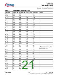
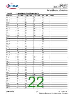
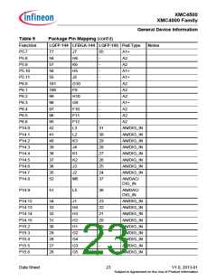
Table 9
Function
P0.0
Package Pin Mapping
LQFP-144 LFBGA-144 LQFP-100 Pad Type
Notes
2
C4
C3
A3
A4
B5
A5
A6
B7
2
A1+
A1+
A2
P0.1
1
1
P0.2
144
143
142
141
140
128
100
99
98
97
96
89
P0.3
A2
P0.4
A2
P0.5
A2
P0.6
A2
P0.7
A2
After a system reset, this
pin selects HW0.
P0.8
127
A8
88
A2
After a system reset, this
pin selects HW0 with a
weak pull-down active.
P0.9
4
D4
B4
E5
D5
C5
4
A2
P0.10
P0.11
P0.12
P0.13
3
3
A1+
A1+
A1+
A1+
139
138
137
95
94
-
Data Sheet
20
V1.0, 2013-01
Subject to Agreement on the Use of Product Information

 INFINEON [ Infineon ]