XMC4500
XMC4000 Family
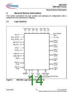
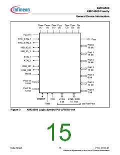
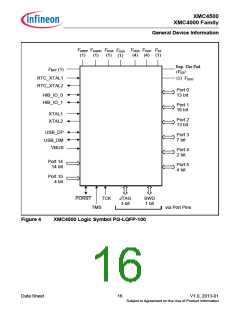
General Device Information
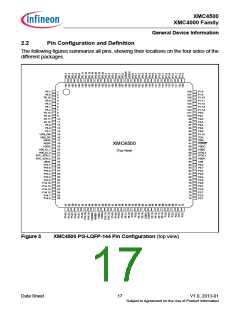
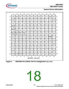
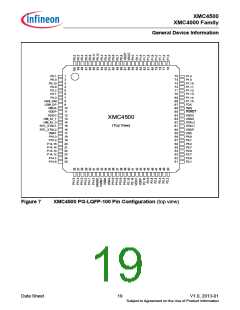
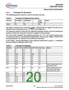
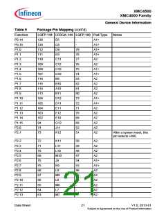
2.2
Pin Configuration and Definition
The following figures summarize all pins, showing their locations on the four sides of the
different packages.
P0.1
P0.0
P0.10
P0.9
P3.2
P3.1
P3.0
P3.13
P3.12
1
2
3
4
5
6
7
8
108
107
106
105
104
103
102
101
100
99
P1.4
P1.5
P1.10
P1.11
P1.12
P1.13
P1.14
P6.0
9
P6.1
P6.2
P3.11
10
11
12
13
14
15
16
17
18
19
20
21
22
23
24
25
26
27
28
29
30
31
32
33
34
35
36
P3.10
P3.9
P3.8
P3.7
98
97
96
95
94
93
92
91
90
89
88
87
86
85
84
83
82
81
80
79
78
77
76
75
P6.3
P6.4
P6.5
P6.6
P1.15
TCK
TMS
PORST
VDDC
VSSO
XTAL2
XTAL1
VDDP
VSS
P5.0
P5.1
P5.2
P5.3
P5.4
P5.5
P5.6
P5.7
P2.6
P2.7
P2.0
P2.1
USB_DM
USB_DP
VBUS
VDDP
VDDC
HIB_IO_1
HIB_IO_0
RTC_XTAL1
RTC_XTAL2
VBAT
XMC4500
(Top View)
P15.7
P15.6
P15.5
P15.4
P15.3
P15.2
P14.15
P14.14
P14.13
P14.12
P14.7
74
73
P14.6
Figure 5
XMC4500 PG-LQFP-144 Pin Configuration (top view)
Data Sheet
17
V1.0, 2013-01
Subject to Agreement on the Use of Product Information

 INFINEON [ Infineon ]