XMC4500
XMC4000 Family
Package and Reliability
4
Package and Reliability
The XMC4500 is a member of the XMC4000 Family of microcontrollers. It is also
compatible to a certain extent with members of similar families or subfamilies.
Each package is optimized for the device it houses. Therefore, there may be slight
differences between packages of the same pin-count but for different device types. In
particular, the size of the Exposed Die Pad may vary.
If different device types are considered or planned for an application, it must be ensured
that the board layout fits all packages under consideration.
4.1
Package Parameters
Table 61 provides the thermal characteristics of the packages used in XMC4500.
Table 61
Thermal Characteristics of the Packages
Symbol Limit Values Unit
Min. Max.
Parameter
Package Types
Exposed Die Pad
Dimensions
Ex × Ey
CC
-
-
-
-
-
6.5 × 6.5 mm
7.0 × 7.0 mm
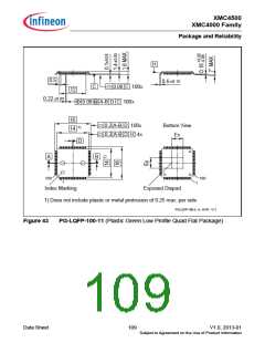
PG-LQFP-144-18
PG-LQFP-100-11
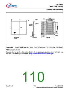
PG-LFBGA-144-10
PG-LQFP-144-181)
PG-LQFP-100-111)
Thermal resistance
Junction-Ambient
RΘJA
CC
40.5
22.4
23.0
K/W
K/W
K/W
1) Device mounted on a 4-layer JEDEC board (JESD 51-7) with thermal vias; exposed pad soldered.
Note: For electrical reasons, it is required to connect the exposed pad to the board
ground VSS, independent of EMC and thermal requirements.
4.1.1
Thermal Considerations
When operating the XMC4500 in a system, the total heat generated in the chip must be
dissipated to the ambient environment to prevent overheating and the resulting thermal
damage.
The maximum heat that can be dissipated depends on the package and its integration
into the target board. The “Thermal resistance RΘJA” quantifies these parameters. The
power dissipation must be limited so that the average junction temperature does not
exceed 150 °C.
The difference between junction temperature and ambient temperature is determined by
ΔT = (PINT + PIOSTAT + PIODYN) × RΘJA
The internal power consumption is defined as
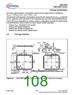
P
INT = VDDP × IDDP (switching current and leakage current).
Data Sheet
107
V1.0, 2013-01
Subject to Agreement on the Use of Product Information

 INFINEON [ Infineon ]